GENERAL DESCRIPTION 
The ADG1438 and ADG1439 are CMOS analog matrix switches with a serially controlled 3-wire interface. The ADG1438 is an 8-channel matrix switch, and the ADG1439 is a dual 4-channel matrix switch.
The ADG1438/ADG1439 use a versatile 3-wire serial interface that operates at clock rates of up to 50 MHz and is compatible with standard SPI, QSPI™, MICROWIRE™, and DSP interface standards. The output of the shift register, SDO, enables a number of the ADG1438/ADG1439 devices to be daisy-chained. On power-up, the internal shift register contains all zeros, and all switches are in the off state.
Each switch conducts equally well in both directions when on, making these devices suitable for both multiplexing and demultiplexing applications. Because each switch is turned on or off by a separate bit, these devices can also be configured as a type of switch array, where any, all, or none of the eight switches can be closed at any time. The input signal range extends to the supply rails. All channels exhibit break-before-make switching action, preventing momentary shorting when switching channels.
The ultralow on resistance and on-resistance flatness of these switches make them ideal solutions for data acquisition and gain switching applications where low distortion is critical. iCMOS® construction ensures ultralow power dissipation, making the parts ideally suited for portable and battery powered instruments.
CARACTÉRISTIQUES
Serial interface up to 50 MHz
SDO daisy-chaining option
9.5 Ω on resistance at 25°C
1.6 Ω on-resistance flatness
Fully specified at ±15 V/+12 V/±5 V
Entrées compatibles avec la logique 3 V
Opération rail à rail
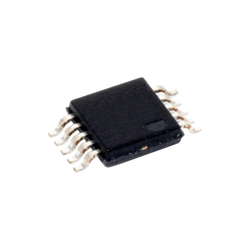
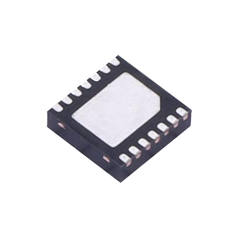
20-lead TSSOP and 20-lead, 4 mm × 4 mm LFCSP
CANDIDATURES
Remplacement du relais
Audio and video routing
Équipement d'essai automatique
Systèmes d'acquisition de données
Temperature measurement systems
Avionique
Systèmes alimentés par batterie
Systèmes de communication
Medical equipment
POINTS FORTS DU PRODUIT
- 50 MHz serial interface.
- 9.5 Ω on resistance.
- 1.6 Ω on-resistance flatness.
- 3 V logic-compatible digital input, VINH = 2.0 V, VINL = 0.8 V.
THÉORIE DU FONCTIONNEMENT
The ADG1438 and ADG1439 are serially controlled, 8-channel and dual 4-channel matrix switches, respectively. While providing the normal multiplexing and demultiplexing functions, these devices also provide the user with more flexibility as to where a signal can be routed. Each of the eight bits of the 8-bit write corresponds to one switch of the device. Logic 1 in a particular bit position turns the switch on, whereas Logic 0 turns the switch off. Because each switch is independently controlled by an individual bit, this provides the option of having any, all, or none of the switches on. This feature may be particularly useful in the demultiplexing application where the user may wish to direct one signal from the drain to a number of outputs (sources). Care must be taken, however, in the multiplexing situation where a number of inputs may be shorted together (separated only by the small on resistance of the switch).
INTERFACE SÉRIE
The ADG1438/ADG1439 has a 3-wire serial interface (SYNC, SCLK, and DIN pins) that is compatible with SPI, QSPI, and MICROWIRE interface standards, as well as most DSPs (see Figure 3 for a timing diagram of a typical write sequence).
The write sequence begins by bringing the SYNC line low. This enables the input shift register. Data from the DIN line is clocked into the 8-bit input shift register on the falling edge of SCLK. The serial clock frequency can be as high as 50 MHz, making the ADG1438/ADG1439 compatible with high speed DSPs.
Data can be written to the shift register in more or fewer than eight bits. In each case, the shift register retains the last eight bits that are written. When all eight bits are written into the shift register, the SYNC line is brought high again. The switches are updated with the new configuration, and the input shift register is disabled. With SYNC held high, the input shift register is disabled so that further data or noise on the DIN line has no effect on the shift register.
Data appears on the SDO pin on the rising edge of SCLK, suitable for daisy-chaining or readback, delayed by eight bits.