Description :
The ADM7172ACPZ is a CMOS, low dropout linear regulator (LDO) that operates from 2.3 V to 6.5 V and provides up to 2 A of output current. This high output current LDO is ideal for regulation of high performance analog and mixed-signal circuits operating from 6 V down to 1.2 V rails. Using an advanced proprietary architecture, the device provides high power supply rejection and low noise, and achieves excellent line and load transient response with just a small 4.7 µF ceramic output capacitor. Load transient response is typically 1.5 μs for a 1 mA to 1.5 A load step.
The ADM7172ACPZ is available in 17 fixed output voltage options. The following voltages are available from stock: 1.3 V, 1.8 V, 2.5 V, 3.0 V, 3.3 V, 4.2 V, and 5.0 V. Additional voltages that are available by special order are: 1.5 V, 1.85 V, 2.0 V, 2.2 V, 2.7 V, 2.75 V, 2.8 V, 2.85 V, 3.8 V, and 4.6 V. An adjustable version is also available that allows output voltages that range from 1.2 V to VIN − VDO with an external feedback divider.
Inrush current can be controlled by adjusting the start-up time via the soft start pin. The typical start-up time with a 1 nF soft start capacitor is 1.0 ms.
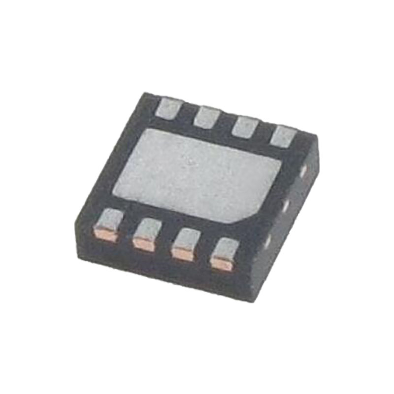
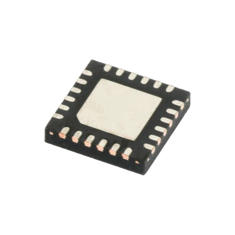
The ADM7172ACPZ regulator output noise is 5 μV rms, independent of the output voltage. The ADM7172 is available in an 8-lead, 3 mm × 3 mm LFCSP, making it not only a very compact solution, but also providing excellent thermal performance for applications requiring up to 2 A of output current in a small, low profile footprint.
Caractéristiques:
Input voltage range: 2.3 V to 6.5 V
Maximum load current: 2 A
Low noise: 5 µV rms independent of output voltage at 100 Hz to 100 kHz
Fast transient response: 1.5 μs for 1 mA to 1.5 A load step
60 dB PSRR at 100 kHz
Low dropout voltage: 172 mV at 2 A load, VOUT = 3 V
Initial accuracy: −0.5% (minimum), +1% (maximum)
Accuracy over line, load, and temperature: ±1.5%
Quiescent current, IGND = 0.7 mA with no load
Low shutdown current: 0.25 μA at VIN = 5 V
Stable with small 4.7 µF ceramic output capacitor
Adjustable and fixed output voltage options: 1.2 V to 5.0 V
Adjustable output from 1.2 V to VIN − VDO
Permettre la précision
Adjustable soft start
Applications :
Regulation to noise sensitive applications: ADC and DAC circuits, precision amplifiers, PLLs/VCOs, and clocking ICs
Communications and infrastructure
Médecine et soins de santé
Industrie et instrumentation
VALEURS MAXIMALES ABSOLUES
| Paramètres | Rating |
| VIN to GND | -0.3Vto +7V |
| VOUTto GND | -0.3V to VIN |
| EN to GND | -0.3Vto +7V |
| SS to GND | -0.3V to VIN |
| SENSE to GND | -0.3Vto +7V |
| Storage TemperatureRange | -65Cto +150°C |
| Operating Junction Temperature Range | -40°C to +125℃ |
| Soldering Conditions | JEDEC J-STD-020 |
Stresses at or above those listed under Absolute Maximum Ratings may cause permanent damage to the product. This is a stress rating only; functional operation of the product at these or any other conditions above those indicated in the operational section of this specification is not implied. Operation beyond the maximum operating conditions for extended periods may affect product reliability
PIN CONFIGURATION AND FUNCTION DESCRIPTIONS
| Pin Function Descriptions: | ||
| Pin No. | Mnemonic | Description |
| 1 | VOUT | Regulated Output Voltage. Bypass this pin to GND with a 4.7 μF or greater capacitor. |
| 2 | VOUT | Regulated Output Voltage. This pin is internally connected to Pin 1. |
| 3 | SENSE | Sense Input. Connect this pin as close as possible to the load for best load regulation.divider to set the output voltage higher than the fixed output voltage. Use an external resistor |
| 4 | SS | Soft Start. A 1 nF external capacitor connected to SS results in a 1.0 ms start-up time. |
| 5 | EN | Regulator Enable. Drive EN high to turn on the regulator; drive EN low to turn off the regulator. For automatic startup, connect EN toVIN(Pin 7 or Pin 8). |
| 6 | GND | Le sol. |
| 7 | VIN | Regulator Input Supply. Bypass this pin to GND with a 4.7μF or greater capacitor. |
| 8 | VIN | Regulator Input Supply. This pin is internally connected to Pin 7. |
| 9 | EP | Exposed Pad. The exposed pad is on the bottom of the package. The exposed pad enhances thermal performance and is electrically connected to GND inside the package. Connect the exposed pad to the ground plane on the board to ensure proper operation. |

