Functional Description
The Cypress CY14B108K/CY14B108M combines a 8-Mbitnonvolatile static RAM (nvSRAM) with a full featured RTC in a monolithic integrated circuit. The embedded nonvolatileelements incorporate QuantumTrap technology producing theworld’s most reliable nonvolatile memory. The SRAM is read andwritten infinite number of times, while independent nonvolatile data resides in the nonvolatile elements.
The RTC function provides an accurate clock with leap year tracking and a programmable, high accuracy oscillator. The alarm function is programmable for periodic minutes, hours, days, or months alarms. There is also a programmable watchdog timer for process control. For a complete list of related documentation.
Caractéristiques
25 ns and 45 ns access times
Internally organized as 1024 K × 8 (CY14B108K)
Hands off automatic STORE on power-down with only a small capacitor
STORE to QuantumTrap nonvolatile elements is initiated by software, device pin, or AutoStore on power-down
RECALL to SRAM initiated by software or power-up
High reliability
Infinite Read, Write, and RECALL cycles
1 million STORE cycles to QuantumTrap
20 year data retention
Single 3 V +20%, –10% operation
Data integrity of Cypress nonvolatile static RAM (nvSRAM) combined with full-featured real time clock (RTC)
Watchdog timer
Clock alarm with programmable interrupts
Capacitor or battery backup for RTC
Industrial temperature
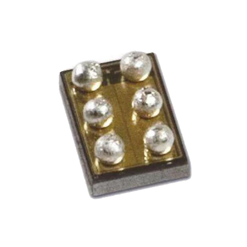
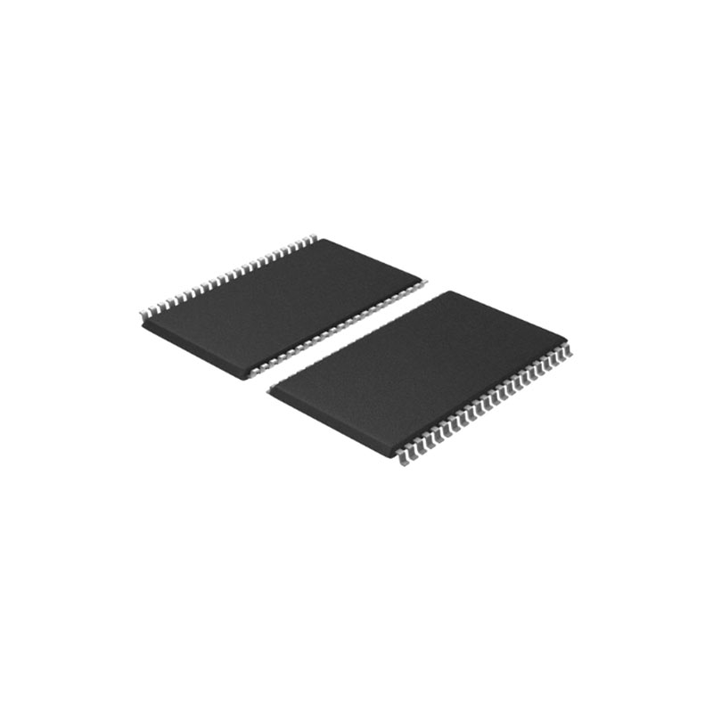
44 and 54-pin thin small outline package (TSOP) Type II
Pb-free and restriction of hazardous substances (RoHS) compliant
Real Time Clock Operation
nvTime Operation
The CY14B108K/CY14B108M offers internal registers thatcontain clock, alarm, watchdog, interrupt, and control functions. RTC registers use the last 16 address locations of the SRAM Internal double buffering of the clock and timer information registers prevents accessing transitional internal clock data during a read or write operation. Double buffering also circumvents disrupting normal timing counts or the clock accuracy of the internal clock when accessing clock data. Clock and alarm registers store data in BCD format.
RTC functionality is described with respect to CY14B108K in the following
The same description applies to CY14B108M, except for the RTC register addresses. The RTC register addresses for CY14B108K range from 0xFFFF0 to 0xFFFFF. Refer to Table 3 on page 15 and Table 4 on page 16 for a detailed Register Map description.
Clock Operations
The clock registers maintain time up to 9,999 years in one-second increments. The time can be set to any calendar time and the clock automatically keeps track of days of the week and month, leap years, and century transitions. There are eight registers dedicated to the clock functions, which are used to set time with a write cycle and to read time with a read cycle. These registers contain the time of day in BCD format. Bits defined as ‘0’ are currently not used and are reserved for future use by Cypress.
Reading the Clock
The double buffered RTC register structure reduces the chance of reading incorrect data from the clock. Internal updates to the CY14B108K time keeping registers are stopped when the read bit ‘R’ (in the Flags register at 0xFFFF0) is set to ‘1’ before reading clock data to prevent reading of data in transition. Stopping the register updates does not affect clock accuracy. When a read sequence of RTC device is initiated, the update of the user timekeeping registers stops and does not restart until a ‘0’ is written to the read bit ‘R’ (in the Flags register at 0xFFFF0).
After the end of read sequence, all the RTC registers are simultaneously updated within 20 ms.
Setting the Clock
A write access to the RTC device stops updates to the time keeping registers and enables the time to be set when the write bit ‘W’ (in the Flags register at 0xFFFF0) is set to ‘1’. The correct day, date, and time is then written into the registers and must be in 24 hour BCD format. The time written is referred to as the “Base Time”. This value is stored in nonvolatile registers and used in the calculation of the current time. When the write bit ‘W’ is cleared by writing ‘0’ to it, the values of timekeeping registers are transferred to the actual clock counters after which the clock resumes normal operation.
If the time written to the timekeeping registers is not in the correct BCD format, each invalid nibble of the RTC registers continue counting to 0xF before rolling over to 0x0 after which RTC resumes normal operation. Note After ‘W’ bit is set to ‘0’, values written into the timekeeping, alarm, calibration, and interrupt registers are transferred to the RTC time keeping counters in tRTCp time. These counter values must be saved to nonvolatile memory either by initiating a Software/Hardware STORE or AutoStore operation. While working in AutoStore disabled mode, perform a STORE operation after tRTCp time while writing into the RTC registers for the modifications to be correctly recorded.