CARACTÉRISTIQUES
Attenuation range: 1 dB LSB steps to 31 dB
Insertion loss: 1.7 dB typical at 3 GHz
Excellent attenuation accuracy: 0.3 dB typical
High Input linearity
0.1dB compression (P0.1dB): 27 dBm typical
Third-order intercept (IP3): 48 dBm typical
High power handling: 27 dBm
Low phase shift: 27°at 3 GHz
Single-supply operation: 3 V to 5 V
CMOS-/TTL-compatible parallel control
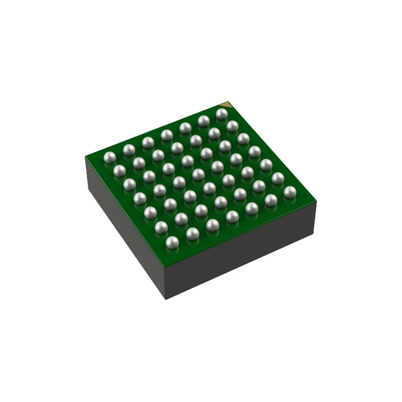
Boîtier LFCSP à 16 pattes, 3 mm × 3 mm
CANDIDATURES
Cellular infrastructure
Microwave radios and very small aperture terminals (VSATs)
Test equipment and sensors
IF and RF designs
DESCRIPTION GÉNÉRALE
The HMC470A is a 5-bit digital attenuator with a 31 dB attenuation control range in 1 dB steps. The HMC470A offers excellent attenuation accuracy and high input linearity over the specified frequency range from 100 MHz to 3 GHz. However, this digital attenuator features ACG pins for external ac grounding capacitors to extend the operation below 100 MHz.
The HMC470A operates with a single positive supply voltage from 3 V to 5 V and provides CMOS-/TTL-compatible parallel control interface by incorporating an on-chip driver. The HMC470A comes in a RoHS compliant, compact, 3 mm × 3 mm LFCSP package.
VALEURS MAXIMALES ABSOLUES
Stresses at or above those listed under Absolute Maximum Ratings may cause permanent damage to the product. This is a stress rating only; functional operation of the product at these or any other conditions above those indicated in the operational section of this specification is not implied. Operation beyond the maximum operating conditions for extended periods may affect product reliability.Only one absolute maximum rating can be applied at any one time.
RÉSISTANCE THERMIQUE
Thermal performance is directly linked to printed circuit board (PCB) design and operating environment. Careful attention to PCB thermal design is required. θJC is the junction to case thermal resistance.
THÉORIE DU FONCTIONNEMENT
The HMC470A incorporates a 5-bit attenuator that offers an attenuation range of 31 dB in 1 dB steps and a driver for CMOS-/TTL-compatible parallel control of the 5-bit attenuator.
POWER SUPPLY
The HMC470A requires a single supply voltage applied to the VDD pin, and CMOS/TTL-compatible control voltages applied to the V1 to V5 pins. The ideal power-up sequence is as follows:
- Connect the ground reference.
- Power up VDD and VSS. The relative order is not important.
- Apply the digital control inputs. The relative order of the digital control inputs is not important.
- Apply an RF input signal to RF1 or RF2.
The power-down sequence is the reverse of the power-up sequence.
RF INPUT AND OUTPUT
The HMC470A is bidirectional. The RF1 and RF2 pins are internally matched to 50 Ω; therefore, they do not require external matching components. These pins are dc-coupled to VDD; therefore, dc blocking capacitors are required on RF lines.
ACGx PINS
The HMC470A is a positive bias GaAs attenuator so it requires floating capacitors between the attenuator bits and ground. The HMC470A uses on-chip floating capacitors that are sufficient for operation at frequencies greater than 700 MHz. The HMC470A also features the ACGx pins to externally connect larger floatingcapacitors. Select the value of external floating capacitors based on the minimum operating frequency, whereas the ACGx pins can be left open when operating above 700 MHz.
EVALUATION BOARD
The HMC470A uses a 4-layer evaluation board. The copper thickness is 0.5 oz (0.7 mil) on each layer. The top dielectric material is 10 mil Rogers RO4350 for optimal high frequency performance,whereas the middle and bottom dielectric materials are FR-4 type materials to achieve an overall board thickness of 62 mil. RF and DC traces are routed on the top copper layer. The bottom and middle layers are grounded planes that provide a solid ground for the RF transmission lines. The RF transmission lines are designed using a coplanar waveguide (CPWG) model with a width of 16 mil and ground spacing of 13 mil to have a characteristic impedance of 50 Ω. For enhanced RF and thermal grounding, as many plated through vias as possible are arranged around transmission lines and under the exposed pad of the package.