DESCRIPTION
The LTC2873 is a robust pin-configurable multiprotocol transceiver that supports RS232, RS485, and RS422 protocols while operating on a single 3V to 5.5V supply. The LTC2873 can be configured as a half-duplex RS485 transceiver or as an RS232 transceiver using the same two bus pins.
A pin-controlled integrated termination resistor allows for easy interface reconfiguration, eliminating external resistors and control relays. Loopback mode steers the driver inputs to the receiver outputs for diagnostic self-test. The RS485 receiver supports up to 256 nodes per bus, and features full failsafe operation for floating, shorted or terminated inputs.
An integrated DC/DC boost converter uses a tiny 2mm × 1.6mm inductor and one capacitor, eliminating the need for multiple supplies when driving RS232 levels.
CARACTÉRISTIQUES
One RS485 or One RS232 Transceiver
3V to 5.5V Supply Voltage
Up to 20Mbps RS485
Slew-Controlled RS232 Operation:
Selectable 1Mbps or 250kbps
Automatic Selection of Integrated RS485 (120Ω) and RS232 (5kΩ) Termination Resistors
High ESD: ±26kV HBM
Logic Loopback Mode
1.7V to 5.5V Logic Interface
Supports Up to 256 RS485 Nodes
RS485 Receiver Failsafe Eliminates UART Lockup
H-Grade Available (–40°C to 125°C)
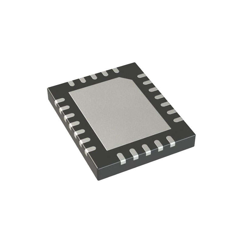
Available in 24-Pin 4mm × 5mm QFN Package
CANDIDATURES
Software Selectable RS232/RS485/RS422 Interface
Industrial Sensors and Actuators
Alarm Systems
Traffic Control and Monitoring
Highway Signs and Jumbo Displays
INFORMATIONS SUR LES APPLICATIONS
The LTC2873 is a flexible multiprotocol transceiver supporting RS485/RS422 and RS232 protocols.
This device can be powered from a single 3V to 5.5V supply with optional logic interface supply as low as 1.7V. An integrated DC/DC converter provides the positive and negative supply rails needed for RS232 operation. Automatically selected integrated termination resistors for both RS232 and RS485 protocols are included, eliminating the need for external termination components and switching relays. A logic loopback control is included for self-test and debug.
The LTC2873 bus interface is a single two-pin port that can be configured as either an RS232 driver/receiver pair or a differential RS485 (and RS422) transceiver depending on the state of the 485/232 pin. In RS485 mode, the driver and receiver can be enabled independently with the DE485/F232 and RE485 pins, or by tying these signals together, a single control selects transmit or receive modes. A 120Ω termination resistor is automatically engaged between pins A/DO and B/RI in RS485 mode if TE485 is low.
Convertisseur DC/DC
The on-chip DC/DC converter operates from the VCC input, generating a 7.0V VDD supply and a charge pumped –6.3V VEE supply, as shown in Figure 16. VDD and VEE power the output stage of the RS232 drivers and are regulated to levels that guarantee greater than ±5V output swing.
Running with External VDD and VEE Supplies
The inductor and charge pump cap, C1, can be omitted only if VDD and VEE are externally supplied. Bypass caps on VDD and VEE must remain in place. In this circumstance, ground the SW pin and float the CAP pin. External supplies must not exceed the absolute maximum levels of ±7.5V. Ideal supply levels are 7.2V and –6.5V as these are each just wider than the regulation points of 7.0V and –6.3V so the internal feedback is satisfied and the switching stops. Lower voltages can be used even at –6V and +6V but the internal boost regulator will be switching. This may cause some switching noise but will not harm the part. VDD and VEE supplies must be present for proper operation in RS232 mode and in RS485 mode when the termination is enabled. It is okay to run the LTC2873 in RS485 mode with internal termination disabled (TE485 high), when VDD and VEE are not present or fully settled.
Inrush Current and Supply Overshoot Precaution
In certain applications, fast supply slew rates are generated when power is connected. If the VCC voltage is greater than 4.5V and its rise time is faster than 10µs, the pins VDD and SW can exceed their absolute maximum values during start-up. When supply voltage is applied to VCC, the voltage difference between VCC and VDD generates inrush current flowing through inductor L1 and capacitors C1 and C2. The peak inrush current must not exceed 2A. To avoid this condition, add a 1Ω resistor as shown in Figure 17. This precaution is not relevant for supply voltages below 4.5V or rise times longer than 10µs.