DESCRIPTION GÉNÉRALE
The AD8476 is a very low power, fully differential precision amplifier with integrated gain resistors for unity gain. It is an ideal choice for driving low power, high performance ADCs as a single-ended-to-differential or differential-to-differential amplifier. It provides a precision gain of 1, common-mode level shifting, low temperature drift, and rail-to-rail outputs for maximum dynamic range.
L'AD8476 fournit également une protection contre les surtensions à partir de grandes tensions d'entrée industrielles jusqu'à ±23 V tout en fonctionnant sur une double alimentation de 5 V. La dissipation de puissance sur une seule alimentation de 5 V est de seulement 1,5 mW. La dissipation de puissance sur une seule alimentation de 5 V est seulement de 1,5 mW.
The AD8476 works well with SAR, Σ-Δ, and pipeline converters. The high current output stage of the part allows it to drive the switched capacitor front-end circuits of many ADCs with minimal error. Unlike many differential drivers on the market, the AD8476 is a high precision amplifier. With 200 µV maximum output offset, 39 nV/√Hz noise, and −102 dB THD + N at 10 kHz, the AD8476 pairs well with low power, high accuracy converters. Considering its low power consumption and high precision, the slew-enhanced AD8476 has excellent speed, settling to 16-bit
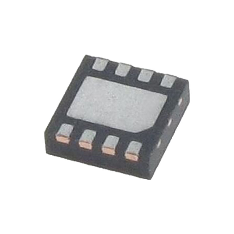
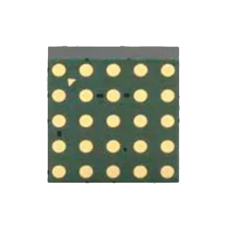
pour des temps d'acquisition de 250 kSPS. L'AD8476 est disponible en boîtiers LFCSP à 16 pattes, 3 mm × 3 mm et MSOP à 8 pattes, peu encombrants. Il est entièrement spécifié sur la plage de température de -40°C à +125°C.
CARACTÉRISTIQUES
Très faible consommation
330 μA courant d'alimentation
Distorsion harmonique extrêmement faible
-126 HD2 à 10 kHz
-128 HD3 à 10 kHz
Entrées/sorties entièrement différentielles ou asymétriques
Sortie différentielle conçue pour piloter des ADC de précision
Pilote les condensateurs commutés et les ADC Σ-Δ
Sorties rail à rail
La broche VOCM ajuste le mode commun de la sortie
Surtension robuste jusqu'à 18 V au-delà des alimentations
Haute performance
Convient pour piloter un convertisseur 16 bits jusqu'à 250 kSPS
39 nV/√Hz bruit de sortie
1 ppm/°C dérive maximale du gain
200 μV décalage maximal de la sortie
10 V/μs vitesse de balayage
Largeur de bande de 6 MHz
Alimentation unique : 3 V à 18 V
Deux alimentations : ±1,5 V à ±9 V
CANDIDATURES
Pilote ADC
Bloc de construction d'un amplificateur différentiel d'instrumentation
Convertisseur asymétrique/différentiel
Instruments alimentés par piles
INFORMATIONS SUR LES APPLICATIONS
CONFIGURATION TYPIQUE
The AD8476 is designed to facilitate single-ended-to-differential conversion, common-mode level shifting, and precision processing of signals so that they are compatible with low voltage ADCs. Figure 54 shows a typical connection diagram of the AD8476. SINGLE-ENDED-TO-DIFFERENTIAL CONVERSION Many industrial systems have single-ended inputs from input sensors; however, the signals are frequently processed by high performance differential input ADCs for higher precision. The AD8476 performs the critical function of precisely converting single-ended signals to the differential inputs of precision ADCs, and it does so with no need for external components. To convert a single-ended signal to a differential signal, connect one input to the signal source and the other input to ground (see Figure 54). Note that either input can be driven by the source with the only effect being that the outputs have reversed polarity. The AD8476 also accepts truly differential input signals in precision systems with differential signal paths.
RÉGLAGE DE LA TENSION EN MODE COMMUN DE LA SORTIE
The VOCM pin of the AD8476 is internally biased by a precision voltage divider comprising of two 1 MΩ resistors between the supplies. This divider level shifts the output to midsupply. Relying on the internal bias results in an output common-mode voltage that is within 0.05% of the expected value. In cases where control of the output common-mode level is desired, an external source or resistor divider can be used to drive the VOCM pin. If driven directly from a source, or with a resistor divider of unequal resistor values, the resistance seen by the VOCM pin should be less than 1 kΩ. If an external voltage divider consisting of equal resistor values is used to set VOCM to midsupply, higher values can be used because the external resistors are placed in parallel with theinternal resistors. The output common-mode offset listed in the Specifications section assumes that the VOCM input is driven by a low impedance voltage source. Because of the internal divider, the VOCM pin sources and sinks current, depending on the externally applied voltage and its associated source resistance. It is also possible to connect the VOCM input to the commonmode level output of an ADC; however, care must be taken to ensure that the output has sufficient drive capability. The input impedance of the VOCM pin is 500 kΩ. If multiple AD8476devices share one ADC reference output, a buffer may be necessary to drive the parallel inputs.