DESCRIPTION
The LTM8055/LTM8055-1 is a 36VIN, buck-boost μModule® (micromodule) regulator. Included in the package are the switching controller, power switches, inductor and support components. A resistor to set the switching frequency, a resistor divider to set the output voltage, and input and output capacitors are all that are needed to complete the design. Other features such as input and output average current regulation may be implemented with just a few components. The LTM8055/LTM8055-1 operates over an input voltage range of 5V to 36V, and can regulate output voltages between 1.2V and 36V. The SYNC input and CLKOUT output allow easy synchronization.
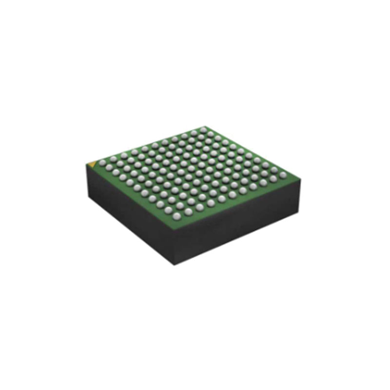
The LTM8055/LTM8055-1 is housed in a compact overmolded ball grid array (BGA) package suitable for automated assembly by standard surface mount equipment.The LTM8055/LTM8055-1 is RoHS compliant.
CARACTÉRISTIQUES
Complete Buck-Boost Switch Mode Power Supply
VOUT Equal, Greater, Less Than VIN
Wide Input Voltage Range: 5V to 36V
12V/3A Output from 6VIN
12V/6A Output from 12VIN
12V/8.5A Output from 24VIN
Up to 97.5% Efficient
Adjustable Input and Output Average Current Limits
Input and Output Current Monitors
Parallelable for Increased Output Current
Wide Output Voltage Range: 1.2V to 36V
Selectable Switching Frequency: 100kHz to 800kHz
Synchronization from 200kHz to 700kHz
External Compensation (LTM8055-1)
15mm × 15mm × 4.92mm BGA Package
CANDIDATURES
High Power Battery-Operated Devices
Industrial Control
Solar Powered Voltage Regulator
Solar Powered Battery Charging
FONCTIONNEMENT
The LTM8055/LTM8055-1 is a standalone nonisolated buck-boost switching DC/DC power supply. The buck-boost topology allows the LTM8055/LTM8055-1 to regulate its output voltage for input voltages both above and below the magnitude of the output. The maximum output current depends upon the input voltage. Higher input voltages yield higher maximum output current.
This converter provides a precisely regulated output voltage programmable via an external resistor divider from 1.2V to 36V. The input voltage range is 5V to 36V, but the LTM8055/LTM8055-1 may be operated at lower input voltages if SVIN is powered by a voltage source above 5V.
The LTM8055/LTM8055-1 contains a current mode controller,power switching elements, power inductor and a modest amount of input and output capacitance.The LTM8055/LTM8055-1 is a fixed frequency PWM regulator.The switching frequency is set by connecting the appropriate
resistor value from the RT pin to GND.
The output voltage of the LTM8055/LTM8055-1 is set by connecting the FB pin to a resistor divider between VOUT and GND.
In addition to regulating its output voltage, the LTM8055/LTM8055-1 is equipped with average current control loops for both the input and output. Add a current sense resistor between IIN and VIN to limit the input current below some maximum value. The IINMON pin reflects the current flowing though the sense resistor between IIN and VIN.
A current sense resistor between VOUT and IOUT allows the LTM8055/LTM8055-1 to accurately regulate its output current to a maximum value set by the value of the sense resistor. When the resistor is present, the IOUTMON pin reflects the output current flowing through VOUT.
In general, the LTM8055/LTM8055-1 should be used with an output sense resistor to limit the maximum output current, as buck-boost regulators are capable of delivering large currents when the output voltage is lower than the input, if demanded.
Furthermore, while the LTM8055/LTM8055-1 does not require an output sense resistor to operate, it uses information from the sense resistor to optimize its performance. If an out-put sense resistor is not used, the efficiency or output ripple may degrade, especially if the current through the integrated inductor is discontinuous. In some cases, an output sense resistor is required to adequately protect the LTM8055/LTM8055-1 against output overload or short-circuit.
A voltage less than 1.2V applied to the CTL pin reduces the maximum output current. Drive CTL to about 50mV to stop switching. The current flowing through the sense resistor is reflected by the output voltage of the IOUTMON pin.
Driving the SYNC pin will synchronize the LTM8055/LTM8055-1 to an external clock source. The CLKOUT pin sources a signal that is the same frequency but approximately 180°out of phase with the internal oscillator.
If more output current is required than a single LTM8055/LTM8055-1 can provide, multiple devices may be operated in parallel.
An internal regulator provides power to the control circuitry and the gate driver to the power MOSFETs. This internal regulator draws power from the SVIN pin. The RUN pin is used to place the LTM8055/LTM8055-1 in shutdown,disconnecting the output and reducing the input current
to less than 1μA.
The LTM8055/LTM8055-1 is equipped with a thermal shutdown that inhibits power switching at high junction temperatures. The activation threshold of this function is above 125°C to avoid interfering with normal operation, so prolonged or repetitive operation under a condition in which the thermal shutdown activates may damage or impair the reliability of the device.
The LTM8055 features an integrated compensation network that works well under most conditions. Some applications, however, benefit from a different compensation network. In such cases, use the LTM8055-1, which has no internal compensation network. Apply an appropriate externalcompensation network for optimal and proper operation.