DESCRIPTION
LTM8083 is a 36VIN, buck-boost μModule regulator. Included in the package is the switching controller, the power switches, an inductor, and support components. All that is needed to complete the design is resistors for setting the output voltage and operating frequency, and input and output capacitors. Operating over an input voltage range from 3V to 36V, the LTM8083 can regulate output voltages between 1V and 36V with seamless low noise transitions between operation regions, as well as controlling both input and output average currents through external sense resistors.
The low profile package enables utilization of unused space on the bottom of PC boards for high density pointof- load regulation. The LTM8083 is packaged in thermally enhanced, compact over-molded Ball Grid Array (BGA) package suitable for automated assembly by standard surface mount equipment. The LTM8083 is RoHS compliant.
CARACTÉRISTIQUES
Complete Buck-Boost Switch Mode Power Supply
Wide Input Voltage Range: 3V to 36V
Wide Output Voltage Range: 1V to 36V
12V/0.8A Output at 6VIN
12V/1.5A Output at 12VIN
12V/1.5A Output at 36VIN
Integrated Three-Terminal Capacitors and Spread Spectrum for Excellent EMI Performance
Compliant with CISPR25 Class 5 Limits (Refer to Figure 25)
300kHz to 2MHz Fixed Switching Frequency with External Frequency Synchronization
Adjustable Output Current Limit
Output Current Monitoring
RoHS Compliant Package
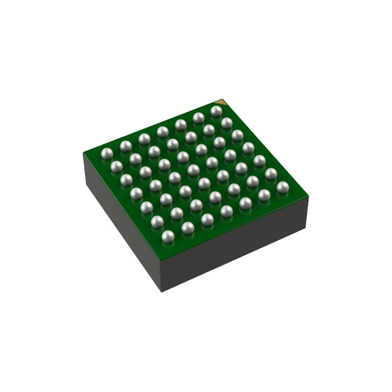
6.25mm × 6.25mm × 2.22mm BGA Package
CANDIDATURES
Battery-Operated Devices
Test and Measurement Equipment
Industrial Control
Solar-Powered Voltage Regulator
Solar-Powered Battery Charging
FONCTIONNEMENT
The LTM8083 is a standalone nonisolated buck-boost switching DC/DC power supply. The buck-boost topology allows the LTM8083 to regulate its output voltage below or above input voltage. Maximum output current is determined by the input voltage. Higher input voltages yield higher maximum output current.
The LTM8083 contains ADI’s proprietary peak-buck peakboost current mode controller with four internal low resistance N-channel DMOS switches, power inductor and a modest amount of input and output capacitors.
This control scheme directly senses the inductor current across the internal power switches and provides smooth transition between buck region, buck-boost region and boost region. A simplified block diagram is given on the previous page. A precisely regulated output voltage is programmable via an external resistor divider from 1V to 36V. The input voltage range is from 3V to 36V.
The LTM8083 is a fixed frequency PWM regulator. A resistor from RT pin to GND sets the switching frequency from 300kHz to 2MHz, allowing applications to be optimized for broad area and efficiency. Driving the SYNC pin will synchronize the LTM8083 to an external clock source.
In addition to the voltage control loop, the LTM8083 is equipped with average current control loop for the output. Add a current sense resistor between ISP and ISN to limit the output current below the maximum value set by the CTRL pin. The ISMON pin reflects the current flowing through the sense resistor.
A voltage less than 1.35V applied to the CTRL pin reduces the maximum output current. The current flowing through the sense resistor is reflected by the voltage of the ISMON pin. Drive CTRL pin below 0.2V to stop switching.
At light load, the LTM8083 typically runs at its switching frequency in discontinuous conduction mode. Both buck and boost reverse current sense thresholds are set to be zero, thus preventing any reverse current flowing from the output to the input.
As the load becomes lower and lower, the LTM8083 may run in pulse-skipping mode, where the switches are held off for multiple cycles (i.e., skipping pulses) to maintain the regulation.
The LTM8083 enters shutdown mode with less than 0.9μA quiescent current when the EN/UVLO pin is below its shutdown threshold (0.3V minimum).
The LTM8083 is equipped with a thermal shutdown that inhibits operation when junction temperature is above 165°C. Prolonged or repetitive operation at junction temperature higher than 125°C may damage or impair the reliability of the device.
A low-ESL 10nF three-terminal capacitor is added on the input side as well as output side, improving noise decoupling for better EMI performance. With a small filter and Spread Spectrum function enabled, the LTM8083 module passes CISPR25 Class 5 conducted and radiated EMI standards.