Description générale
The MCP4725 is a low-power, high accuracy, single channel, 12-bit buffered voltage output Digital-to Analog Converter (DAC) with nonvolatile memory (EEPROM). Its on-board precision output amplifier allows it to achieve rail-to-rail analog output swing.
The DAC input and configuration data can be programmed to the nonvolatile memory (EEPROM) by the user using I2C interface command. The nonvolatile memory feature enables the DAC device to hold the DAC input code during power-off time, and the DAC output is available immediately after power-up. This feature is very useful when the DAC device is used as a supporting device for other devices in the network.
The device includes a Power-on-Reset (POR) circuit to ensure reliable power-up and an on-board charge pump for the EEPROM programming voltage. The DAC reference is driven from VDD directly. In powerdown mode, the output amplifier can be configured to present a known low, medium, or high resistance output load.
The MCP4725 has an external A0 address bit selection pin. This A0 pin can be tied to VDD or VSS of the user’s application board.
The MCP4725 has a two-wire I2C compatible serial interface for standard (100 kHz), fast (400 kHz), or high speed (3.4 MHz) mode.
The MCP4725 is an ideal DAC device where design simplicity and small footprint is desired, and for applications requiring the DAC device settings to be saved during power-off time.
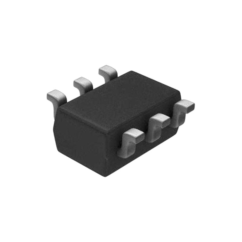
The device is available in a small 6-pin SOT-23 and DFN package.
Caractéristiques
• 12-Bit Resolution
• On-Board Nonvolatile Memory (EEPROM)
• ±0.2 LSB DNL (typical)
• External A0 Address Pin
• Normal or Power-Down Mode
• Fast Settling Time: 6 µs (typical)
• External Voltage Reference (VDD)
• Rail-to-Rail Output
• Low Power Consumption
• Single-Supply Operation: 2.7V to 5.5V
• I²C Interface:
– Eight Available Addresses
– Standard (100 kbps), Fast (400 kbps), and High-Speed (3.4 Mbps) Modes
• Small 6-Lead SOT-23 and DFN Package Options
• Extended Temperature Range: -40°C to +125°C
Applications
• Set Point or Offset Trimming
• Sensor Calibration
• Closed-Loop Servo Control
• Low Power Portable Instrumentation
• PC Peripherals
• Data Acquisition Systems
Analog Output Voltage (VOUT)
VOUT is an analog output voltage from the DAC device. The DAC output amplifier drives this pin with a range of VSS to VDD.
Supply Voltage (VDD or VSS)
VDD is the power supply pin for the device. The voltage at the VDD pin is used as the supply input as well as the DAC reference input. The power supply at the VDD pin should be as clean as possible for good DAC performance.
This pin requires an appropriate bypass capacitor of about 0.1 µF (ceramic) to ground. An additional 10 µF capacitor (tantalum) in parallel is also recommended to further attenuate high frequency noise present in application boards. The supply voltage (VDD) must be maintained in the 2.7V to 5.5V range for specified operation.
VSS is the ground pin and the current return path of the device. The VSS pin must be connected to a ground plane through a low impedance connection. If an analog ground path is available in the application PCB (printed circuit board), it is highly recommended that the VSS pin be tied to the analog ground path or isolated within an analog ground plane of the circuit board.
Serial Clock Pin (SCL)
SCL is the serial clock pin of the I²C interface. The MCP4725 acts only as a slave and the SCL pin accepts only external serial clocks. The input data from the Master device is shifted into the SDA pin on the rising edges of the SCL clock and output from the MCP4725 occurs at the falling edges of the SCL clock. The SCL pin is an open-drain N-channel driver. Therefore, it needs a pull-up resistor from the VDD line to the SCL pin.