DETAILED DESCRIPTION
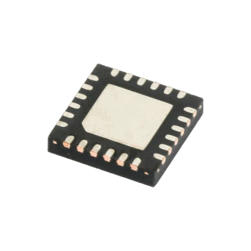
The DS1302 trickle-charge timekeeping chip contains a real-time clock/calendar and 31 bytes of static RAM. It communicates with a microprocessor via a simple serial interface. The real-time clock/calendar provides seconds, minutes, hours, day, date, month, and year information. The end of the month date is automatically adjusted for months with fewer than 31 days, including corrections for leap year. The clock operates in either the 24-hour or 12-hour format with an AM/PM indicator.
Interfacing the DS1302 with a microprocessor is simplified by using synchronous serial communication. Only three wires are required to communicate with the clock/RAM: CE, I/O (data line), and SCLK (serial clock). Data can be transferred to and from the clock/RAM 1 byte at a time or in a burst of up to 31 bytes. The DS1302 is designed to operate on very low power and retain data and clock information on less than 1µW.
The DS1302 is the successor to the DS1202. In addition to the basic timekeeping functions of the DS1202, the DS1302 has the additional features of dual power pins for primary and backup power supplies, programmable trickle charger for VCC1, and seven additional bytes of scratchpad memory.
Data Description
CE AND CLOCK CONTROL
Driving the CE input high initiates all data transfers. The CE input serves two functions. First, CE turns on the control logic that allows access to the shift register for the address/command sequence. Second, the CE signal provides a method of terminating either single-byte or multiple-byte CE data transfer.
A clock cycle is a sequence of a rising edge followed by a falling edge. For data inputs, data must be valid during the rising edge of the clock and data bits are output on the falling edge of clock. If the CE input is low, all data transfer terminates and the I/O pin goes to a high-impedance state. DATA INPUT
Following the eight SCLK cycles that input a write command byte, a data byte is input on the rising edge of the next eight SCLK cycles. Additional SCLK cycles are ignored should they inadvertently occur. Data is input starting with bit 0.
DATA OUTPUT
Following the eight SCLK cycles that input a read command byte, a data byte is output on the falling edge of the next eight SCLK cycles. Note that the first data bit to be transmitted occurs on the first falling edge after the last bit of the command byte is written. Additional SCLK cycles retransmit the data bytes should they inadvertently occur so long as CE remains high. This operation permits continuous burst mode read capability. Also, the I/O pin is tri stated upon each rising edge of SCLK. Data is output starting with bit 0.
BURST MODE
Burst mode can be specified for either the clock/calendar or the RAM registers by addressing location 31 decimal (address/command bits 1 through 5 = logic 1). As before, bit 6 specifies clock or RAM and bit 0 specifies read or write. There is no data storage capacity at locations 9 through 31 in the Clock/Calendar Registers or location 31 in the RAM registers. Reads or writes in burst mode start with bit 0 of address 0.
When writing to the clock registers in the burst mode, the first eight registers must be written in order for the data to be transferred. However, when writing to RAM in burst mode it is not necessary to write all 31 bytes for the data to transfer. Each byte that is written to will be transferred to RAM regardless of whether all 31 bytes are written or not.
CLOCK/CALENDAR
The time and calendar information is obtained by reading the appropriate register bytes. Table 3 illustrates the RTC registers. The time and calendar are set or initialized by writing the appropriate register bytes. The contents of the time and calendar registers are in the binary-coded decimal (BCD) format.
The day-of-week register increments at midnight. Values that correspond to the day of week are user-defined but must be sequential (i.e., if 1 equals Sunday, then 2 equals Monday, and so on.). Illogical time and date entries result in undefined operation.
When reading or writing the time and date registers, secondary (user) buffers are used to prevent errors when the internal registers update. When reading the time and date registers, the user buffers are synchronized to the internal registers the rising edge of CE.
The countdown chain is reset whenever the seconds register is written. Write transfers occur on the falling edge of CE. To avoid rollover issues, once the countdown chain is reset, the remaining time and date registers must be written within 1 second.
The DS1302 can be run in either 12-hour or 24-hour mode. Bit 7 of the hours register is defined as the 12- or 24-hour mode-select bit. When high, the 12-hour mode is selected. In the 12-hour mode, bit 5 is the AM/PM bit with logic high being PM. In the 24-hour mode, bit 5 is the second 10-hour bit (20–23 hours). The hours data must be re-initialized whenever the 12/24 bit is changed.

