説明
The LT3758/LT3758A are wide input range, current mode, DC/DC controllers which are capable of generating either positive or negative output voltages. They can be configured as either a boost, flyback, SEPIC or inverting converter. The LT3758/LT3758A drive a low side external N-channel power MOSFET from an internal regulated 7.2V supply. The fixed frequency, current-mode architecture results in stable operation over a wide range of supply and output voltages.
The operating frequency of LT3758/LT3758A can be set with an external resistor over a 100kHz to 1MHz range, and can be synchronized to an external clock using the SYNC pin. A minimum operating supply voltage of 5.5V, and a low shutdown quiescent current of less than 1μA, make the LT3758/LT3758A ideally suited for batterypowered systems.
The LT3758/LT3758A feature soft-start and frequency foldback functions to limit inductor current during startup and output short-circuit. The LT3758A has improved load transient performance compared to the LT3758.
特徴
Wide Input Voltage Range: 5.5V to 100V
Positive or Negative Output Voltage Programming with a Single Feedback Pin
Current Mode Control Provides Excellent Transient Response
Programmable Operating Frequency (100kHz to 1MHz) with One External Resistor
Synchronizable to an External Clock
Low Shutdown Current < 1μA
Internal 7.2V Low Dropout Voltage Regulator
Programmable Input Undervoltage Lockout with Hysteresis
プログラム可能なソフトスタート
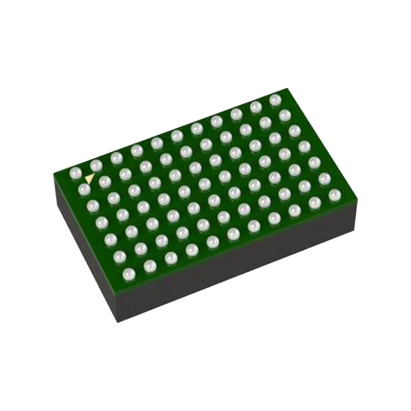
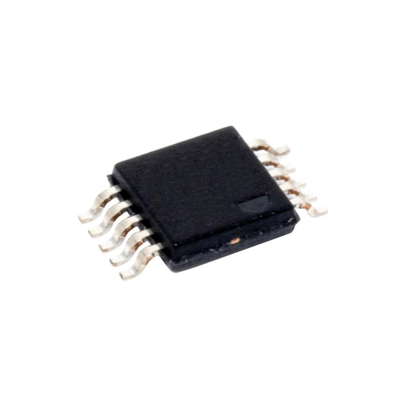
Small 10-Lead DFN (3mm × 3mm) and MSOPE Packages
自動車用AEC-Q100認定
アプリケーション
自動車
テレコム
インダストリアル
アプリケーション情報
Main Control Loop
The LT3758 uses a fixed frequency, current mode control scheme to provide excellent line and load regulation. Operation can be best understood by referring to the Block Diagram.
The start of each oscillator cycle sets the SR latch (SR1) and turns on the external power MOSFET switch M1 through driver G2. The switch current flows through the external current sensing resistor RSENSE and generates a voltage proportional to the switch current. This current sense voltage VISENSE (amplified by A5) is added to a stabilizing slope compensation ramp and the resulting sum (SLOPE) is fed into the positive terminal of the PWM comparator A7. When SLOPE exceeds the level at the negative input of A7 (VC pin), SR1 is reset, turning off the power switch. The level at the negative input of A7 is set by the error amplifier A1 (or A2) and is an amplified version of the difference between the feedback voltage (FBX pin) and the reference voltage (1.6V or –0.8V, depending on the configuration). In this manner, the error amplifier sets the correct peak switch current level to keep the output in regulation.
The LT3758 has a switch current limit function. The current sense voltage is input to the current limit comparator A6. If the SENSE pin voltage is higher than the sense current limit threshold VSENSE(MAX) (110mV, typical), A6 will reset SR1 and turn off M1 immediately.
The LT3758 is capable of generating either positive or negative output voltage with a single FBX pin. It can be configured as a boost, flyback or SEPIC converter to generate positive output voltage, or as an inverting converter to generate negative output voltage. When configured as a SEPIC converter, the FBX pin is pulled up to the internal bias voltage of 1.6V by a voltage divider (R1 and R2) connected from VOUT to GND. Comparator A2 becomes inactive and comparator A1 performs the inverting amplification from FBX to VC. When the LT3758 is in an inverting configuration, the FBX pin is pulled down to –0.8V by a voltage divider connected from VOUT to GND. Comparator A1 becomes inactive and comparator A2 performs the noninverting amplification from FBX to VC.
The LT3758 has overvoltage protection functions to protect the converter from excessive output voltage overshoot during start-up or recovery from a short-circuit condition. An overvoltage comparator A11 (with 20mV hysteresis) senses when the FBX pin voltage exceeds the positive regulated voltage (1.6V) by 8% and provides a reset pulse. Similarly, an overvoltage comparator A12 (with 10mV hysteresis) senses when the FBX pin voltage exceeds the negative regulated voltage (–0.8V) by 11% and provides a reset pulse. Both reset pulses are sent to the main RS latch (SR1) through G6 and G5. The power MOSFET switch M1 is actively held off for the duration of an output overvoltage condition.