説明
The 5P49V6965 is a programmable clock generator intended for high-performance consumer, networking, industrial, computing, and data-communications applications. Configurations may be stored in on-chip One-Time Programmable (OTP) memory or changed using I2C interface. This is Renesas’ sixth generation of programmable clock technology (VersaClock 6E).
The frequencies are generated from a single reference clock. The reference clock can come from one of the two redundant clock inputs. A glitchless manual switchover function allows one of the redundant clocks to be selected during normal operation.
Two select pins allow up to four different configurations to be programmed and accessible using processor GPIOs or bootstrapping. The different selections may be used for different operating modes (full function, partial function, partial power-down), regional standards (US, Japan, Europe) or system production margin testing. The device may be configured to use one of two I2C addresses to allow multiple devices to be used in a system.
代表的なアプリケーション
Ethernet switch/router
PCI Express 1.0 / 2.0 / 3.0 / 4.0 Spread Spectrum on
PCI Express 1.0 / 2.0 / 3.0 / 4.0 / 5.0 Spread Spectrum off
Broadcast video/audio timing
Multi-function printer
Processor and FPGA clocking
Any-frequency clock conversion
MSAN/DSLAM/PON
Fiber Channel, SAN
Telecom line cards
Laser distance sensing
特徴
Flexible 1.8V, 2.5V, 3.3V power-rails
High-performance, low phase noise PLL, < 0.5ps RMS typical phase jitter on outputs
Four banks of internal OTP memory
In-system or factory programmable
2 select pins accessible with processor GPIOs or bootstrapping
I²C serial programming interface
0xD0 or 0xD4 I2C address options allows multiple devices configured in a same system
Reference LVCMOS output clock
Four universal output pairs individually configurable:
Differential (LVPECL, LVDS or HCSL)
2 single-ended (2 LVCMOS in-phase or 180 degrees out of phase)
I/O VDDs can be mixed and matched, supporting 1.8V (LVDS and LVCMOS), 2.5V, or 3.3V
Output frequency ranges:
LVCMOS clock outputs: 1kHz to 200MHz
LVDS, LVPECL, HCSL differential clock outputs: 1kHz to 350MHz
Redundant clock inputs with manual switchover
Programmable output enable or power-down mode
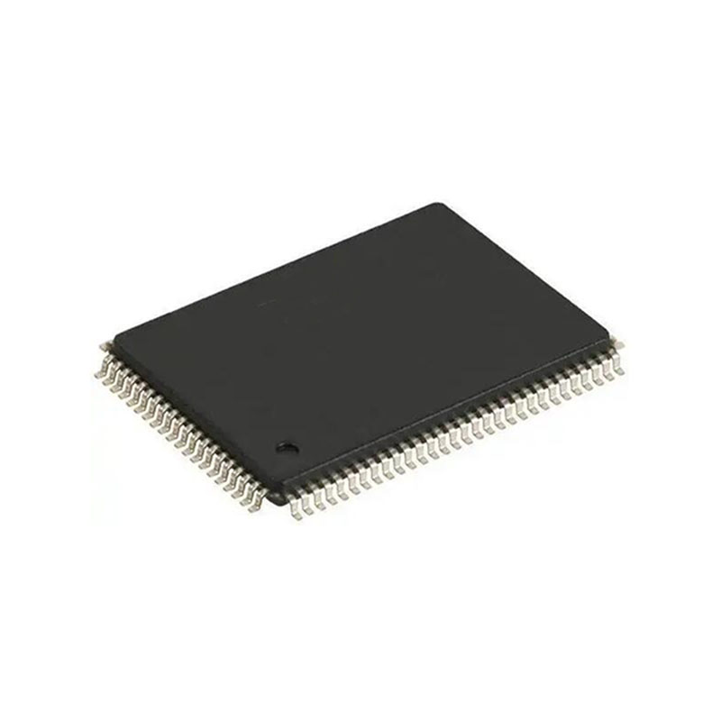
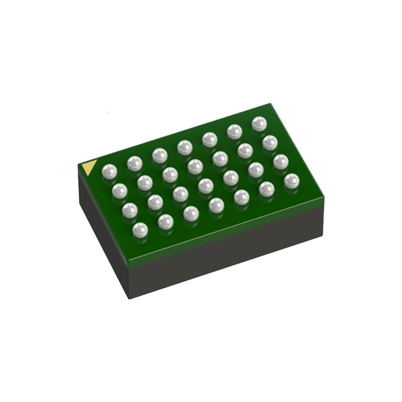
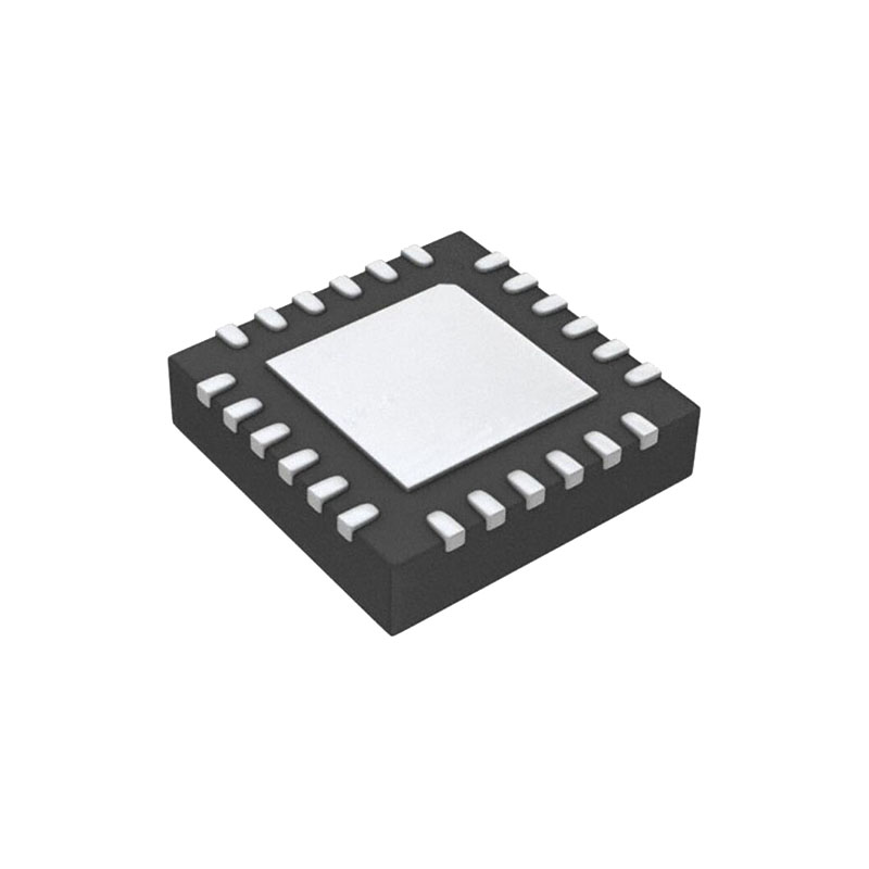
Available in 4 × 4 mm 24-VFQFPN package
-40° to +85°C industrial temperature operation
Features and Functional Blocks
Device Startup and Power-On-Reset
The device has an internal power-up reset (POR) circuit. All VDDs must be connected to desired supply voltage to trigger POR.
User can define specific default configurations through internal One-Time-Programmable (OTP) memory. Either customer or factory can program the default configuration. Please refer to VersaClock 6E Family Register Descriptions and Programming Guide for details.
Device will identity which of the 2 modes to operate in by the state of OUT0_SEL_I2CB pin at POR. Both of the 2 modes default configurations can be programmed as stated above.
- Software Mode (I2C): OUT0_SEL_I2CB is low at POR. I2C interface will be open to users for in-system programming, overriding device default configurations at any time.
- Hardware Select Mode: OUT0_SEL_I2CB is high at POR. Device has been programmed to load OTP at power-up (REG0[7]=1). The device will load internal registers according to Table 19. Power-up Behavior. Internal OTP memory can support up to 4 configurations, selectable by SEL0/SEL1 pins. At POR, logic levels at SEL0 and SEL1 pins must be settled, resulting the selected configuration to be loaded at power up. After the first 10ms of operation, the levels of the SELx pins can be changed, either to low or to the same level as VDDD/VDDA. The SELx pins must be driven with a digital signal of < 300ns rise/fall time and only a single pin can be changed at a time. After a pin level change, the device must not be interrupted for at least 1ms so that the new values have time to load and take effect.
Reference Clock and Selection
The device supports up to two clock inputs.
Crystal input, can be driven by a single-ended clock.
Clock input (CLKIN, CLKINB), a fully differential input that only accepts a reference clock. A single-ended clock can also drive it on CLKIN.