概要
The AD8605, AD8606, and AD86081 are single, dual, and quad rail-to-rail input and output, single-supply amplifiers. They feature very low offset voltage, low input voltage and current noise, and wide signal bandwidth. They use the Analog Devices, Inc. patented DigiTrim trimming technique, which achieves superior precision without laser trimming.
The combination of low offsets, low noise, very low input bias currents, and high speed makes these amplifiers useful in a wide variety of applications. Filters, integrators, photodiode amplifiers, and high impedance sensors all benefit from the combination of performance features. Audio and other ac applications benefit from the wide bandwidth and low distortion. Applications for these amplifiers include optical control loops, portable and loop-powered instrumentation, and audio amplification for portable devices.
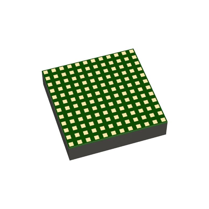
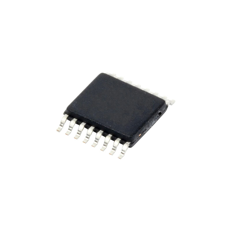
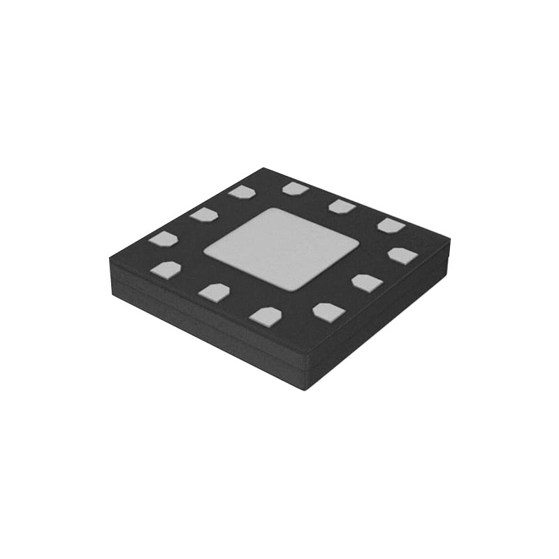
The AD8605, AD8606, and AD8608 are specified over the extended industrial temperature range (−40°C to +125°C). The AD8605 single is available in 5-lead SOT-23 and 5-ball WLCSP packages. The AD8606 dual is available in an 8-lead MSOP, an 8-ball WLSCP, and a narrow SOIC surface-mounted package. The AD8608 quad is available in a 14-lead TSSOP package and a narrow 14-lead SOIC package. The 5-ball and 8-ball WLCSP offer the smallest available footprint for any surface-mounted operational amplifier. The WLCSP, SOT-23, MSOP, and TSSOP versions are available in tape-and-reel only.
特徴
Low offset voltage: 65 μV maximum
Low input bias currents: 1 pA maximum
Low noise: 8 nV/√Hz
Wide bandwidth: 10 MHz
High open-loop gain: 1000 V/mV
Unity gain stable
単一電源動作:2.7V~5.5V
5-ball WLCSP for single (AD8605) and 8-ball WLCSP for dual (AD8606)
アプリケーション
Photodiode amplification
バッテリー駆動の計測器
多極フィルター
センサー
バーコードスキャナー
オーディオ
アプリケーション情報
OUTPUT PHASE REVERSAL
Phase reversal is defined as a change in polarity at the output of the amplifier when a voltage that exceeds the maximum input common-mode voltage drives the input.
Phase reversal can cause permanent damage to the amplifier; it can also cause system lockups in feedback loops. The AD8605 does not exhibit phase reversal even for inputs exceeding the supply voltage by more than 2 V.
最大消費電力
Power dissipated in an IC causes the die temperature to increase, which can affect the behavior of the IC and the application circuit performance.
The absolute maximum junction temperature of the AD8605/ AD8606/AD8608 is 150°C. Exceeding this temperature could damage or destroy the device.
INPUT OVERVOLTAGE PROTECTION The AD860x has internal protective circuitry. However, if the voltage applied at either input exceeds the supplies by more than 0.5 V, external resistors should be placed in series with the inputs.
The remarkable low input offset current of the AD860x (<1 pA) allows the use of larger value resistors. With a 10 kΩ resistor at the input, the output voltage has less than 10 nV of error voltage. A 10 kΩ resistor has less than 13 nV/√Hz of thermal noise at room temperature.
THD + NOISE
Total harmonic distortion is the ratio of the input signal in V rms to the total harmonics in V rms throughout the spectrum. Harmonic distortion adds errors to precision measurements and adds unpleasant sonic artifacts to audio systems.
The AD860x has a low total harmonic distortion.The AD8605 is configured in positive unity gain, which is the worst case, and with a load of 10 kΩ.
CHANNEL SEPARATION
Channel separation, or inverse crosstalk, is a measure of the signal feed from one amplifier (channel) to another on the same IC.
The AD8606 has a channel separation of greater than −160 dB up to frequencies of 1 MHz, allowing the two amplifiers to amplify ac signals independently in most applications.
CAPACITIVE LOAD DRIVE
The AD860x can drive large capacitive loads without oscillation. In this case, the amplifier is configured in positive unity gain, worst case for stability, while driving a 1000 pF load at its output. Driving larger capacitive loads in unity gain can require the use of additional circuitry.
A snubber network, helps reduce the signal overshoot to a minimum and maintain stability. Although this circuit does not recover the loss of bandwidth induced by large capacitive loads, it greatly reduces the overshoot and ringing. This method does not reduce the maximum output swing of the amplifier.