概要
The AD9249 is a 16-channel, 14-bit, 65 MSPS analog-to-digital converter (ADC) with an on-chip sample-and-hold circuit that is designed for low cost, low power, small size, and ease of use. The device operates at a conversion rate of up to 65 MSPS and is optimized for outstanding dynamic performance and low power in applications where a small package size is critical.
The ADC requires a single 1.8 V power supply and an LVPECL-/ CMOS-/LVDS-compatible sample rate clock for full performance operation. No external reference or driver components are required for many applications.
The AD9249 automatically multiplies the sample rate clock for the appropriate LVDS serial data rate. Data clock outputs (DCO±1, DCO±2) for capturing data on the output and frame clock outputs (FCO±1, FCO±2) for signaling a new output byte are provided. Individual channel power-down is supported, and the device typically consumes less than 2 mW when all channels are disabled.
The ADC contains several features designed to maximize flexibility and minimize system cost, such as programmable clock and data alignment and programmable digital test pattern generation.
The available digital test patterns include built-in deterministic and pseudorandom patterns, along with custom user-defined test patterns entered via the serial port interface (SPI).
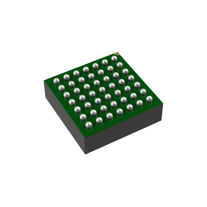
The AD9249 is available in an RoHS-compliant, 144-ball CSPBGA. It is specified over the industrial temperature range of −40°C to +85°C. This product is protected by a U.S. patent.
特徴
低電力
16 ADC channels integrated into 1 package
58 mW per channel at 65 MSPS with scalable power options
35 mW per channel at 20 MSPS
SNR: 75 dBFS (to Nyquist); SFDR: 90 dBc (to Nyquist)
DNL: ±0.6 LSB (typical); INL: ±0.9 LSB (typical)
Crosstalk, worst adjacent channel, 10 MHz, −1 dBFS: −90 dB typical
Serial LVDS (ANSI-644, default)
Low power, reduced signal option (similar to IEEE 1596.3)
Data and frame clock outputs
650 MHz full power analog bandwidth
2 V p-p input voltage range
1.8 V supply operation
Serial port control
Flexible bit orientation
Built in and custom digital test pattern generation
Programmable clock and data alignment
Power-down and standby modes
アプリケーション
Medical imaging
Communications receivers
Multichannel data acquisition
製品ハイライト
Small Footprint. Sixteen ADCs are contained in a small, 10 mm × 10 mm package.
Low Power. 35 mW/channel at 20 MSPS with scalable power options.
Ease of Use. Data clock outputs (DCO±1, DCO±2) operate at frequencies of up to 455 MHz and support double data rate (DDR) operation.
User Flexibility. SPI control offers a wide range of flexible features to meet specific system requirements.
動作理論
The AD9249 is a multistage, pipelined ADC. Each stage provides sufficient overlap to correct for flash errors in the preceding stage. The quantized outputs from each stage are combined into a final 14-bit result in the digital correction logic. The serializer transmits this converted data in a 14-bit output. The pipelined architecture permits the first stage to operate with a new input sample while the remaining stages operate with preceding samples. Sampling occurs on the rising edge of the clock.
Each stage of the pipeline, excluding the last, consists of a low resolution flash ADC connected to a switched capacitor DAC and an interstage residue amplifier (for example, a multiplying digital-to-analog converter (MDAC)). The residue amplifier magnifies the difference between the reconstructed DAC output and the flash input for the next stage in the pipeline. One bit of redundancy is used in each stage to facilitate digital correction of flash errors. The last stage simply consists of a flash ADC.
The output staging block aligns the data, corrects errors, and passes the data to the output buffers. The data is then serialized and aligned to the frame and data clocks.