概要
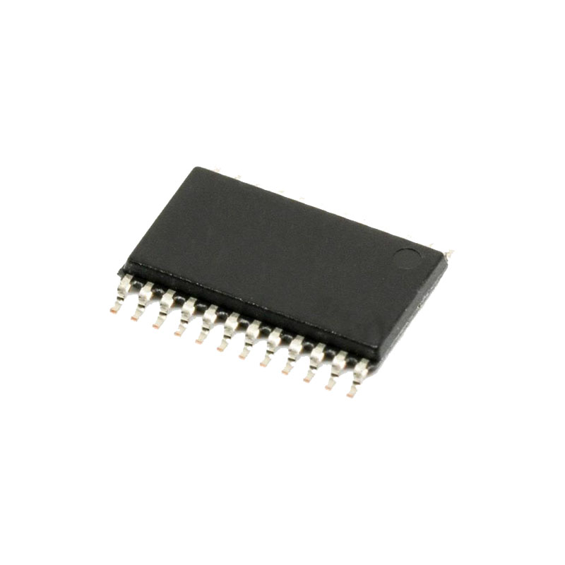
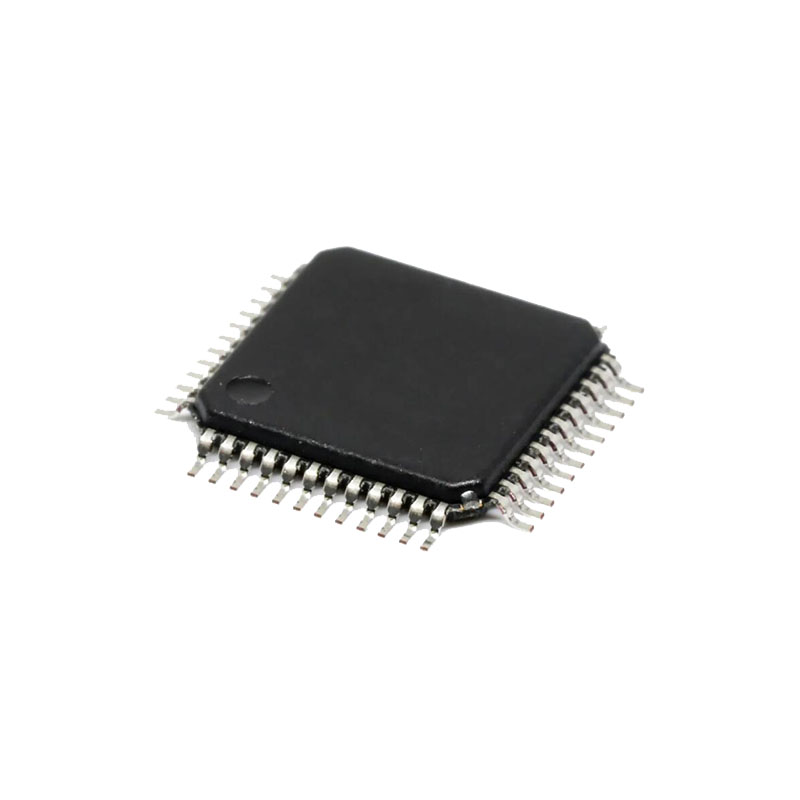
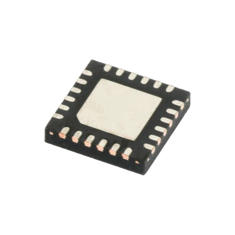
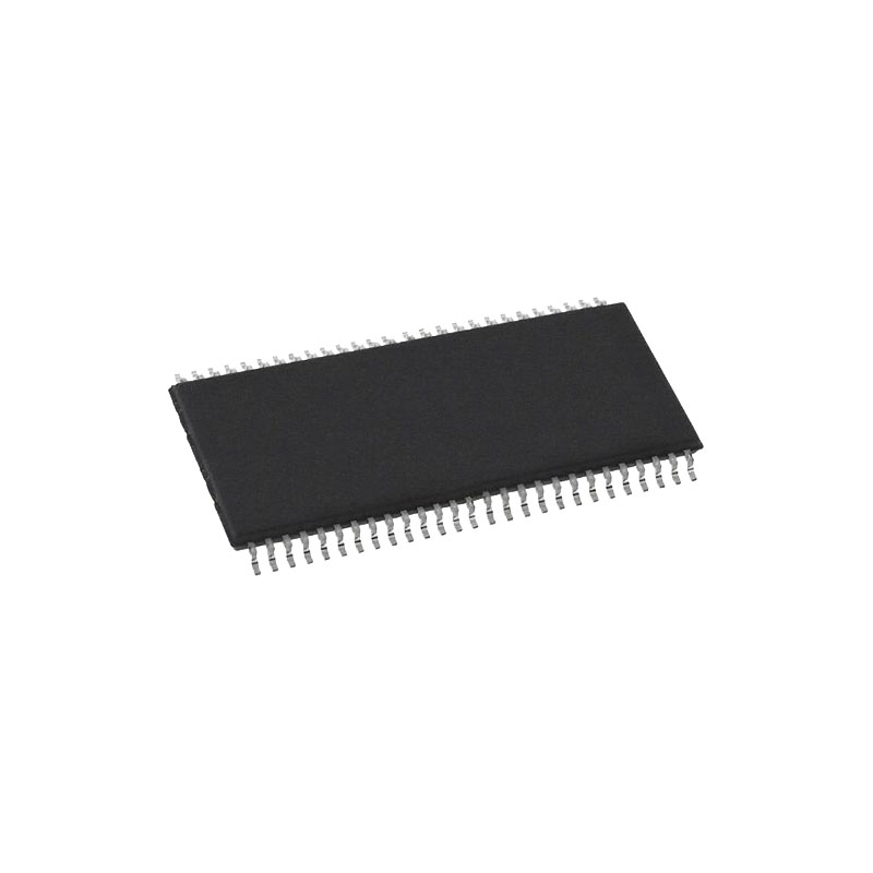
The ADG714/ADG715 are complementary metal-oxide semiconductor (CMOS), octal single-pole, single-throw (SPST) switches, controlled via either a 2- or 3-wire serial interface. On resistance is closely matched between the switches and is flat over the full signal range. Each switch conducts equally well in both directions, and the input signal range extends to the supplies. Data is written to these devices in the form of 8 bits, each bit corresponding to one channel. The ADG714 uses a 3-wire serial interface that is compatible with serial peripheral interface (SPI), QSPI™, MICROWIRE™ interface standards, and most digital signal processing (DSP) interface standards. The output of the shift register DOUT enables a number of these devices to be daisy-chained. The ADG715 uses a 2-wire serial interface that is compatible with the I2C interface standard. The ADG715 has four hardwired addresses, selectable from two external address pins (A0 and A1). The pins allow the two LSBs of the 7-bit slave address to be set by the user. A maximum of four of these devices may be connected to the bus. On power-up of these devices, all switches are in the off condition, and the internal registers contain all zeros. A low power consumption and operating supply range of 2.7 V to 5.5 V make these devices ideal for many applications. These devices can also be supplied from a dual ±2.5 V supply. The ADG714 is available in a 24-lead TSSOP and a 24-lead LFCSP, and the ADG715 is available in a 24-lead TSSOP.
製品ハイライト
1.2- or 3-wire serial interface.
2.Single-/dual-supply operationThe ADG714 and ADG715 are fully specified and guaranteed with 3 V, 5 V, and ±2.5 V supply rails.
3.Low on resistance, typically 2.5 Ω.
4.Low leakage.
5.Power-on reset.
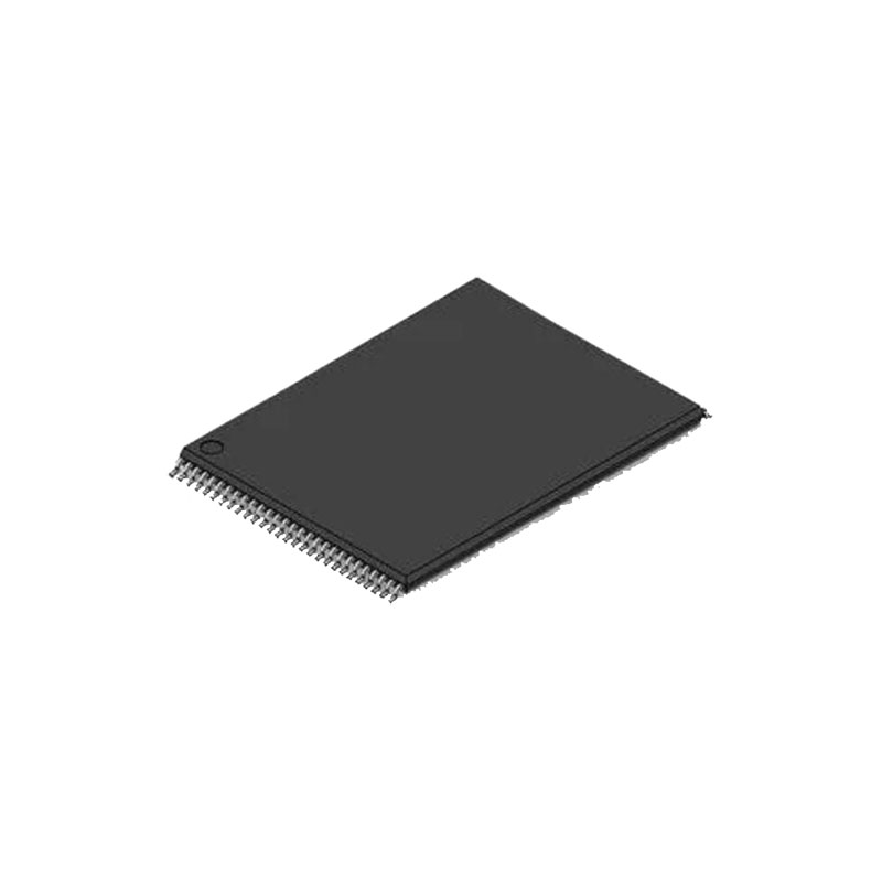
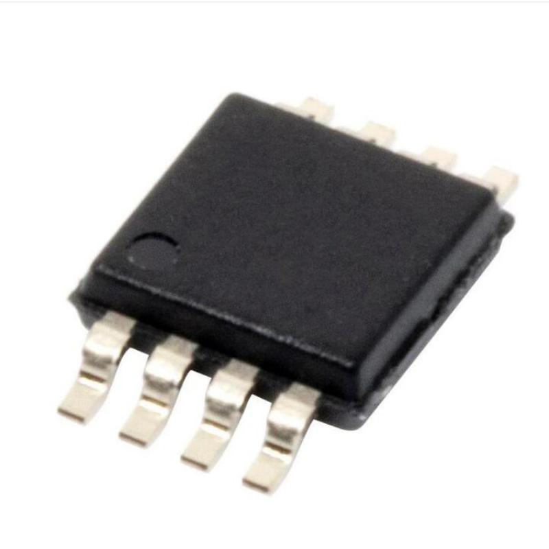
6.A 24-lead TSSOP for both the ADG714 and the ADG715. A 24-lead LFCSP for the ADG714.
特徴
SPI/QSPI/MICROWIRE-compatible interface (ADG714)
ADG715: I2C-compatible interface (ADG715)
2.7 V to 5.5 V single supply
±2.5 V dual supply
2.5 Ω on resistance
0.6 Ω on resistance flatness
0.1 nA leakage currents
Octal SPST
Power-on reset
Fast switching times
TTL/CMOS compatible
24-lead TSSOP and 24-lead LFCSP
アプリケーション
Data acquisition systems
Communication systems
Relay replacement
Audio and video switching
動作理論
The ADG714 and ADG715 are serially controlled, octal SPST switches, controlled by either a 2- or 3-wire interface. Each bit of the 8-bit serial word corresponds to one switch of the device. A Logic 1 in the bit position turns the switch on, and a Logic 0 turns the switch off. Each switch is independently controlled by an individual bit, which provides the option of having any, all, or none of the switches on. When changing the switch conditions, a new 8-bit word is written to the input shift register. Some of the bits may be the same as the previous write cycle because the user may not change the state of some switches. To minimize glitches on the output of these switches, the devices compare the state of switches from the previous write cycle. When the switches are already in the on condition and are required to stay on, there are minimal glitches on the output of the switch.
POWER-ON RESET
On power-up of the device, all switches are in the off condition, the internal shift register is filled with zeros, and the register remains so until a valid write takes place.
Input Shift Register
The input shift register is eight bits wide. Figure 24 illustrates the contents of the input shift register. Data is loaded into the device as an 8-bit word under the control of a serial clock input, SCL. The 8-bit word consists of eight data bits, each controlling one switch. MSB (Bit 7) is loaded first.

