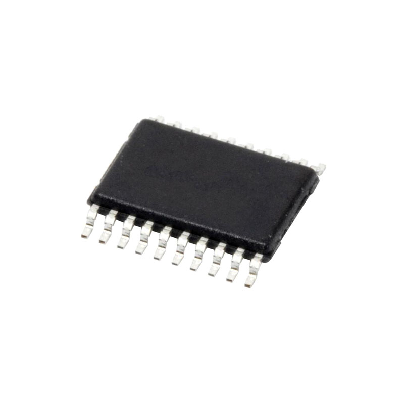
概要
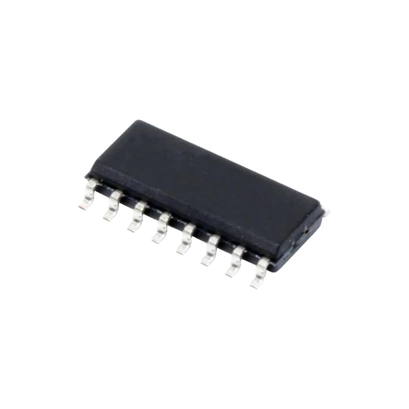
The ADM2582E/ADM2587E are fully integrated signal and power isolated data transceivers with ±15 kV ESD protection and are suitable for high speed communication on multipoint transmission lines. The ADM2582E/ADM2587E include an integrated isolated dc-to-dc power supply, which eliminates the need for an external dc-to-dc isolation block. They are designed for balanced transmission lines and comply with ANSI/TIA/EIA-485-A-98 and ISO 8482:1987(E). The devices integrate Analog Devices, Inc., iCoupler® technology to combine a 3-channel isolator, a three-state differential line driver, a differential input receiver, and Analog Devices isoPower® dc-todc converter into a single package. The devices are powered by a single 5 V or 3.3 V supply, realizing a fully integrated signal and power isolated RS-485 solution. The ADM2582E/ADM2587E driver has an active high enable. An active low receiver enable is also provided, which causes the receiver output to enter a high impedance state when disabled. The devices have current limiting and thermal shutdown features to protect against output short circuits and situations where bus contention may cause excessive power dissipation. The parts are fully specified over the industrial temperature range and are available in a highly integrated, 20-lead, wide-body SOIC package. The ADM2582E/ADM2587E contain isoPower technology that uses high frequency switching elements to transfer power through the transformer. Special care must be taken during printed circuit board (PCB) layout to meet emissions standards. Refer to the AN-0971 Application Note, Control of Radiated Emissions with isoPower Devices, for details on board layout considerations.
特徴
Isolated RS-485/RS-422 transceiver, configurable as half or
full duplex
isoPower integrated isolated dc-to-dc converter
±15 kV ESD protection on RS-485 input/output pins
Complies with ANSI/TIA/EIA-485-A-98 and ISO 8482:1987(E)
ADM2582E data rate: 16 Mbps
ADM2587E data rate: 500 kbps
5 V or 3.3 V operation
Connect up to 256 nodes on one bus
Open- and short-circuit, fail-safe receiver inputs
High common-mode transient immunity: >25 kV/µs
Thermal shutdown protection
安全性と規制当局の承認
UL recognition: 2500 V rms for 1 minute per UL 1577
VDE Certificates of Conformity
DIN EN 60747-5-2 (VDE 0884 Part 2): 2003-01
VIORM = 560 V peak
Operating temperature range: −40°C to +85°C
Highly integrated, 20-lead, wide-body SOIC package
アプリケーション
Isolated RS-485/RS-422 interfaces
Industrial field networks
Multipoint data transmission systems
アプリケーション情報
PCB LAYOUT AND ELECTROMAGNETIC INTERFERENCE (EMI)
The ADM2582E/ADM2587E isolated RS-422/RS-485 transceiver contains an isoPower integrated dc-to-dc converter, requiring no external interface circuitry for the logic interfaces. Power supply bypassing is required at the input and output supply pins . The power supply section of the ADM2582E/ ADM2587E uses a 180 MHz oscillator frequency to pass power efficiently through its chip-scale transformers. In addition, the normal operation of the data section of the iCoupler introduces switching transients on the power supply pins. Bypass capacitors are required for several operating frequencies. Noise suppression requires a low inductance, high frequency capacitor, whereas ripple suppression and proper regulation require a large value capacitor. These capacitors are connected between Pin 1 (GND1) and Pin 2 (VCC) and Pin 8 (VCC) and Pin 9 (GND1) for VCC. The VISOIN and VISOOUT capacitors are connected between Pin 11 (GND2) and Pin 12 (VISOOUT) and Pin 19 (VISOIN) and Pin 20 (GND2). To suppress noise and reduce ripple, a parallel combination of at least two capacitors is required with the smaller of the two capacitors located closest to the device. The recommended capacitor values are 0.1 µF and 10 µF for VISOOUT at Pin 11 and Pin 12 and VCC at Pin 8 and Pin 9. Capacitor values of 0.01 µF and 0.1 µF are recommended for VISOIN at Pin 19 and Pin 20 and VCC at Pin 1 and Pin 2. The recommended best practice is to use a very low inductance ceramic capacitor, or its equivalent, for the smaller value. The total lead length between both ends of the capacitor and the input power supply pin should not exceed 10 mm. The dc-to-dc converter section of the ADM2582E/ADM2587E components must operate, out of necessity, at a very high frequency to allow efficient power transfer through the small transformers. This creates high frequency currents that can propagate in circuit board ground and power planes, causing edge and dipole radiation. The ADM2582E/ADM2587E features an internal split paddle, lead frame on the bus side. For the best noise suppression, filter both the GND2 pins (Pin 11 and Pin 14) and VISOOUT signals of the integrated dc-to-dc converter for high frequency currents. Use surface-mount ferrite beads in series with the signals before routing back to the device. See Figure 35 for the recommended PCB layout. The impedance of the ferrite bead is chosen to be about 2 kΩ between the 100 MHz and 1 GHz frequency range to reduce the emissions at the 180 MHz primary switching ADM2582E/ADM2587E frequency and the 360 MHz secondary side rectifying frequency and harmonics.

