特徴
4 inputs, 1 output HDMI/DVI links
±8 kV ESD protection on input pins
HDMI 1.4a receive and transmit compliant
Supports 250 Mbps to 2.25 Gbps data rates and beyond
Supports 25 MHz to 225 MHz pixel clocks and beyond
Fully buffered unidirectional inputs/outputs
Switchable 50 Ω on-chip input terminations with manual
or automatic control on channel switch
Equalized inputs with low added jitter compensate for
more than 20 meters of HDMI cable at 2.25 Gbps
Loss of signal (LOS) detect circuit on TMDS clock
Output disable feature for reduced power dissipation
Bidirectional DDC buffers (SDA and SCL)
EDID replication reduces component count, while enabling
simultaneous access to all HDMI sources
5 V combiner provides power to EDID replicator and CEC
buffer when local system power is off
Bidirectional buffered CEC line with integrated pull-up
resistors (26 kΩ)
Hot plug detect pulse low on channel switch with
programmable pulse width or direct manual control
Standards compatible: HDMI, DVI, HDCP, I²C
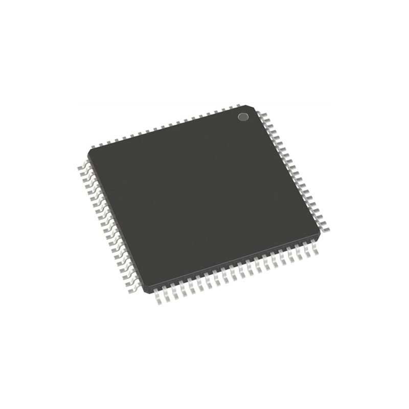
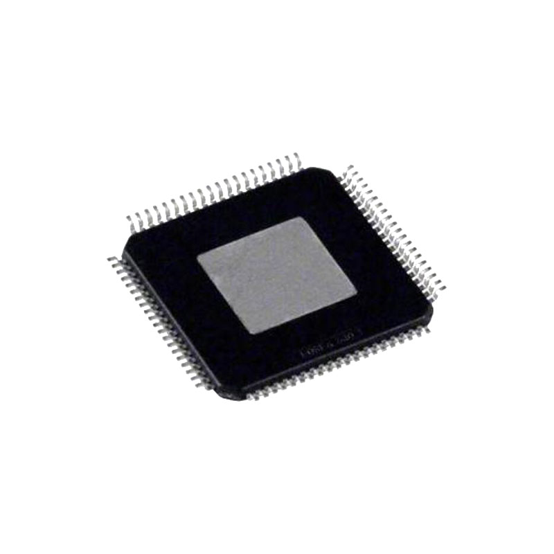
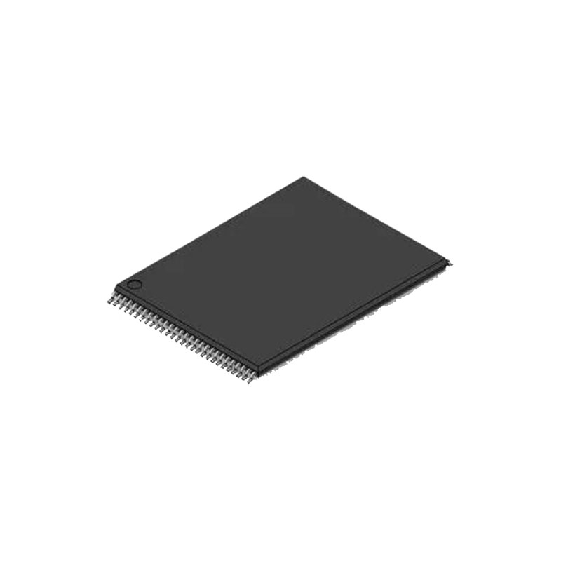
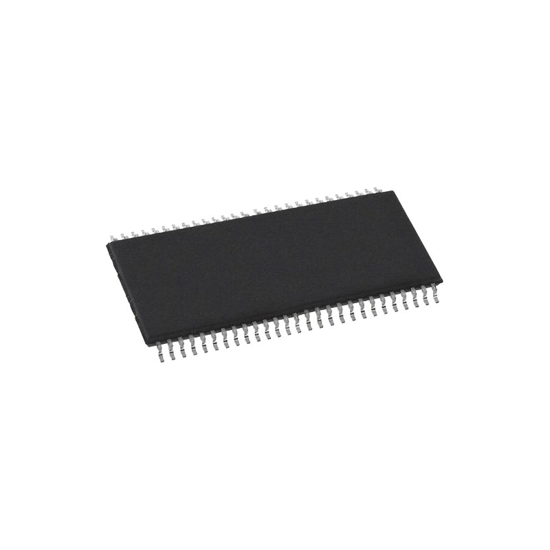
80-lead, 14 mm × 14 mm LQFP RoHS-compliant package
アプリケーション
Advanced television (HDTV) sets
Projectors
A/V receivers
Set-top boxes
概要
The ADV3002 is a complete HDMI™/DVI link switch featuringequalized transition minimized differential signaling (TMDS)inputs, ideal for systems with long cable runs. The ADV3002 includes bidirectional buffering for the DDC bus and CEC line,with integrated pull-up resistors for the CEC line. Additionally,the ADV3002 includes an EDID replication function that enables one EDID EEPROM to be shared for all four HDMI ports.The ADV3002 is provided in a space-saving, 80-lead LQFP surface-mount, Pb-free plastic package and is specified to operate over the 0°C to 85°C temperature range.
製品ハイライト
- Input cable equalizer enables use of long cables at the input.
For a 24 AWG cable, the ADV3002 compensates for more
than 20 meters at data rates of up to 2.25 Gbps.
- Auxiliary multiplexer isolates and buffers the DDC bus and
the CEC line, increasing total system capacitance limit.
- EDID replication eliminates the need for multiple EDID
EEPROMs. EDID can be loaded from a single external
EEPROM or from a system microcontroller.
- 5 V power combiner powers the EDID replicator and CEC
buffer when local system power is off.
- Integrated hot plug detect pulse low on channel switch
with programmable pulse width or direct manual control.
Controlling the Characteristic Impedance of a TMDS Differential Pair
The characteristic impedance of a differential pair depends on a number of variables, including the trace width, the distance between the two traces, the height of the dielectric material between the trace and the reference plane below it, and the dielectric constant of the PCB binder material. To a lesser extent, the characteristic impedance also depends upon the trace thickness and the presence of solder mask. Many combinations can produce the correct characteristic impedance. Generally, working with the PCB fabricator is required to obtain a set of parameters to produce the desired results. One consideration is how to guarantee a differential pair with a differential impedance of 100 Ω over the entire length of the trace. One technique to accomplish this is to change the width of the traces in a differential pair based on how closely one trace is coupled to the other. When the two traces of a differential pair are close and strongly coupled, they should have a width that produces a100 Ω differential impedance. When the traces split apart to go into a connector, for example, and are no longer so strongly coupled, the width of the traces need to be increased to yield a differential impedance of 100 Ω in the new configuration.For more information, please contact us or query the data sheet. Thank you!

