説明
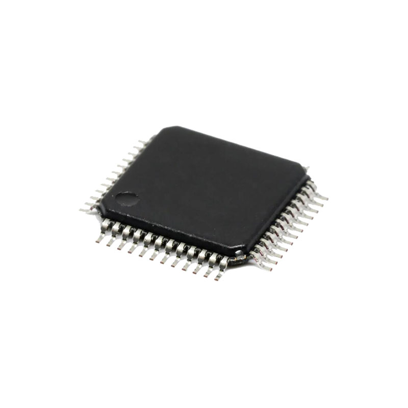
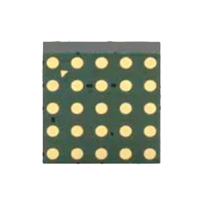
The AT24C256C provides 262,144 bits of Serial Electrically Erasable and Programmable Read-Only Memory (EEPROM) organized as 32,768 words of 8 bits each. The device’s cascading feature allows up to eight devices to share a common two-wire bus. The device is optimized for use in many industrial and commercial applications where low-power and low-voltage operation are essential. The devices are available in space‑saving 8-lead SOIC, 8-lead TSSOP, 8-pad UDFN and 8-ball VFBGA packages. All packages operate from 1.7V to 5.5V.
特徴
• Low-Voltage and Standard-Voltage Operation:
– VCC = 1.7V to 5.5V
• Internally Organized as 32,768 x 8 (256K)
• Industrial Temperature Range: -40°C to +85°C
• I2C-Compatible (Two-Wire) Serial Interface:
– 100 kHz Standard mode, 1.7V to 5.5V
– 400 kHz Fast mode, 1.7V to 5.5V
– 1 MHz Fast Mode Plus (FM+), 2.5V to 5.5V
• Schmitt Triggers, Filtered Inputs for Noise Suppression
• Bidirectional Data Transfer Protocol
• Write-Protect Pin for Full Array Hardware Data Protection
• Ultra Low Active Current (3 mA maximum) and Standby Current (6 μA maximum)
• 64-Byte Page Write Mode:
– Partial page writes allowed
• Random and Sequential Read Modes
• Self-Timed Write Cycle within 5 ms Maximum
• ESD Protection >4,000V
• High Reliability:
– Endurance: 1,000,000 write cycles
– Data retention: 100 years
• Green Package Options (Lead-free/Halide-free/RoHS compliant)
• Die Sale Options: Wafer Form and Bumped Wafers
Device Address Inputs (A0, A1, A2)
The A0, A1 and A2 pins are device address inputs that are hard-wired (directly to GND or to VCC) for compatibility with other two-wire Serial EEPROM devices. When the pins are hard-wired, as many as eight devices may be addressed on a single bus system. A device is selected when a corresponding hardware and software match is true. If these pins are left floating, the A0, A1 and A2 pins will be internally pulled down to GND. However, due to capacitive coupling that may appear in customer applications, Microchip recommends always connecting the address pins to a known state. When using a pull‑up resistor, Microchip recommends using 10 kΩ or less.
Device Operation and Communication
The AT24C256C operates as a client device and utilizes a simple I2C-compatible two-wire digital serial interface to communicate with a host controller, commonly referred to as the bus host. The host initiates and controls all read and write operations to the client devices on the serial bus, and both the host and the client devices can transmit and receive data on the bus.
The serial interface is comprised of just two signal lines: Serial Clock (SCL) and Serial Data (SDA). The SCL pin is used to receive the clock signal from the host, while the bidirectional SDA pin is used to receive command and data information from the host as well as to send data back to the host. Data is always latched into the AT24C256C on the rising edge of SCL and always output from the device on the falling edge of SCL. Both the SCL and SDA pins incorporate integrated spike suppression filters and Schmitt Triggers to minimize the effects of input spikes and bus noise.
All command and data information is transferred with the Most Significant bit (MSb) first. During bus communication, one data bit is transmitted every clock cycle, and after eight bits (one byte) of data have been transferred, the receiving device must respond with either an Acknowledge (ACK) or a No-Acknowledge (NACK) response bit during a ninth clock cycle (ACK/NACK clock cycle) generated by the host. Therefore, nine clock cycles are required for every one byte of data transferred. There are no unused clock cycles during any read or write operation, so there must not be any interruptions or breaks in the data stream during each data byte transfer and ACK or NACK clock cycle.
During data transfers, data on the SDA pin must only change while SCL is low and the data must remain stable while SCL is high. If data on the SDA pin changes while SCL is high, then either a Start or a Stop condition will occur. Start and Stop conditions are used to initiate and end all serial bus communication between the host and the client devices. The number of data bytes transferred between a Start and a Stop condition is not limited and is determined by the host. In order for the serial bus to be idle, both the SCL and SDA pins must be in the logic high state at the same time.