説明
The DAC7568, DAC8168, and DAC8568 are lowpower, voltage-output, eight-channel, 12-, 14-, and 16-bit digital-to-analog converters (DACs), respectively. These devices include a 2.5V, 2ppm/°C internal reference (disabled by default), giving a fullscale output voltage range of 2.5V or 5V. The internal reference has an initial accuracy of 0.004% and can source up to 20mA at the VREFIN/VREFOUT pin. These devices are monotonic, providing excellent linearity and minimizing undesired code-to-code transient voltages (glitch). They use a versatile 3-wire serial interface that operates at clock rates up to 50MHz. The interface is compatible with standard SPI™, QSPI™, Microwire™, and digital signal processor (DSP) interfaces.
The DAC7568, DAC8168, and DAC8568 incorporate a power-on-reset circuit that ensures the DAC output powers up at either zero scale or midscale until a valid code is written to the device. These devices contain a power-down feature, accessed over the serial interface, that reduces current consumption to typically 0.18μA at 5V. Power consumption (including internal reference) is typically 2.9mW at 3V, reducing to less than 1μW in power-down mode. The low power consumption, internal reference, and small footprint make these devices ideal for portable, battery-operated equipment.
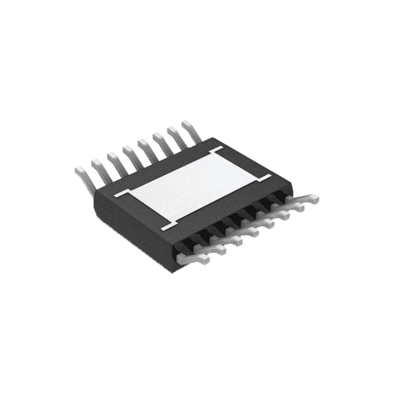
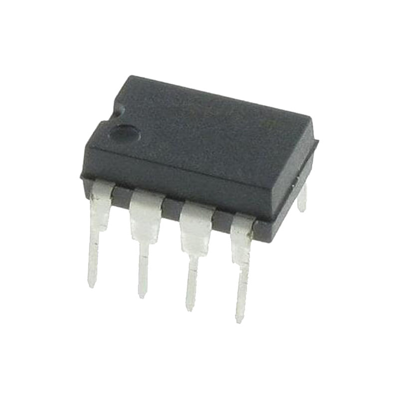
The DAC7568, DAC8168, and DAC8568 are drop-in and function-compatible with each other, and are available in TSSOP-16 and TSSOP-14 packages.
特徴
Relative Accuracy:
– DAC7568 (12-Bit): 0.3 LSB INL
Glitch Energy: 0.1nV-s
Internal Reference:
– 2.5V Reference Voltage (disabled by default)
– 0.004% Initial Accuracy (typ)
– 2ppm/°C Temperature Drift (typ)
– 5ppm/°C Temperature Drift (max)
– 20mA Sink/Source Capability
Power-On Reset to Zero Scale or Midscale
Ultralow Power Operation: 1.25mA at 5V Including Internal Reference Current
Wide Power-Supply Range: +2.7V to +5.5V
Monotonic Over Entire Temperature Range
Low-Power Serial Interface with Schmitt-Triggered Inputs: Up to 50MHz
On-Chip Output Buffer Amplifier with Rail-to-Rail Operation
Temperature Range: –40°C to +125°C
アプリケーション
Portable Instrumentation
Closed-Loop Servo-Control/Process Control
Data Acquisition Systems
Programmable Attenuation, Digital Gain, and Offset Adjustment
Programmable Voltage and Current Sources
Layout
Layout Guidelines
A precision analog component requires careful layout, adequate bypassing, and clean, well-regulated power supplies.
The DAC7568, DAC8168, and DAC8568 offer single-supply operation, and are often used in close proximity with digital logic, microcontrollers, microprocessors, and digital signal processors. The more digital logic present in the design and the higher the switching speed, the more difficult it is to keep digital noise from appearing at the output.
As a result of the single ground pin of the DAC7568, DAC8168, and DAC8568, all return currents (including digital and analog return currents for the DAC) must flow through a single point. Ideally, GND would be connected directly to an analog ground plane. This plane would be separate from the ground connection for the digital components until they were connected at the power-entry point of the system.
The power applied to AVDD should be well-regulated and low noise. Switching power supplies and dc/dc converters often have high-frequency glitches or spikes riding on the output voltage. In addition, digital components can create similar high-frequency spikes as their internal logic switches states. This noise can easily couple into the DAC output voltage through various paths between the power connections and analog output.
As with the GND connection, AVDD should be connected to a power-supply plane or trace that is separate from the connection for digital logic until they are connected at the power-entry point. In addition, a 1μF to 10μF capacitor and 0.1μF bypass capacitor are strongly recommended. In some situations, additional bypassing may be required, such as a 100μF electrolytic capacitor or even a Pi filter made up of inductors
特徴
Internal Reference
The DAC7568, DAC8168, and DAC8568 include a 2.5V internal reference that is disabled by default. The internal reference is externally available at the VREFIN/VREFOUT pin. A minimum 100nF capacitor is recommended between the reference output and GND for noise filtering.
The internal reference of the DAC7568, DAC8168, and DAC8568 is a bipolar, transistor-based, precision bandgap voltage reference. Transistors Q1 and Q2 are biased such that the current density of Q1 is greater than that of Q2. The difference of the two base-emitter voltages (VBE1 – VBE2) has a positive temperature coefficient and is forced across resistor R1. This voltage is gained up and added to the base-emitter voltage of Q2, which has a negative temperature coefficient. The resulting output voltage is virtually independent of temperature. The short-circuit current is limited by design to approximately 100mA.