概要
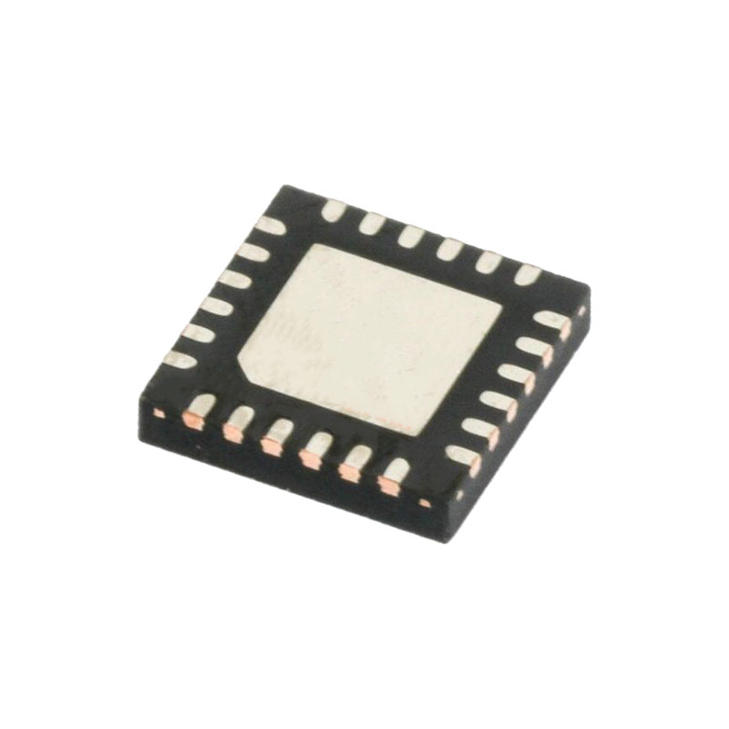
The DS1856M dual, temperature-controlled, nonvolatile (NV) variable resistors with three monitors consists of two 256-position, linear, variable resistors; three analog monitor inputs (MON1, MON2, MON3); and a direct-to-digital temperature sensor. The device provides an ideal method for setting and temperature-compensating bias voltages and currents in control applications using minimal circuitry. The variable resistor settings are stored in EEPROM memory and can be accessed over the 2-wire serial bus.
The DS1856M includes 128 bytes of EEPROM memory at A2h slave address, Table 00/01. The DS1856M also includes three-levels of password protection. The DS1856-01 includes 256 bytes of A0h EEPROM memory. The DS1856B-M50+ and DS1856E-M50+ are drop-in replacements for the DS1856B-050+ and DS1866E-050+, respectively. The enhancements include 256 bytes of EEPROM at A0h; selectable MON2, MON3 references; and a 13-bit ADC. These are backward compatible by default with the DS1856B-050+/DS1856E-050+.
アプリケーション
Optical Transceivers
Optical Transponders
Instrumentation and Industrial Controls
RF Power Amps
Diagnostic Monitoring
特徴
SFF-8472 Compatible
13-Bit ADC
Two Linear, 256-Position, Nonvolatile Temperature-Controlled Variable Resistors with 2°C Resolution
Three Levels of Security
Access to Monitoring and ID Information Configurable with Separate Device Addresses
2-Wire Serial Interface
Two Buffers with TTL/CMOS-Compatible Inputs and Open-Drain Outputs
Operates from a 3.3V or 5V Supply
-40°C to +95°C Operating Temperature Range
詳細
The user can read the registers that monitor the VCC, MON1, MON2, MON3, and temperature analog signals. After each signal conversion, a corresponding bit is set that can be monitored to verify that a conversion has occurred. The signals also have alarm and warning flags that notify the user when the signals go above or below the user-defined value. Interrupts can also be set for each signal.
The position values of each resistor can be independently programmed. The user can assign a unique value to each resistor for every 2°C increment over the-40°C to +102°C range. Two buffers are provided to convert logic-level inputs into open-drain outputs. Typically, these buffers are used to implement transmit (Tx) fault and loss-of-signal (LOS) functionality. Additionally, OUT1 can be asserted in the event that one or more of the monitored values go beyond user-defined limits.
Memory Description
The DS1856M 2-wire interface uses 8-bit addressing, which allows up to 256 bytes to be addressed traditionally on a given 2-wire slave address. However, since the A2h Memory contains more than 256 bytes, a table scheme is used. The lower 128 bytes of the A2h Memory, memory locations 00h to 7Fh, function as expected and are independent of the currently selected table. Byte 7Fh is the Table Select byte. This byte determines which memory table is accessed by the 2wire interface when address locations 80h–FFh are accessed. Memory locations 80h–FFh are accessible only through the A2h Memory address.
Before attempting to read and write any of the bits or bytes mentioned in this section, it is important to look at the memory map provided in a subsequent section to verify what level of password is required.
Page Write
The DS1856M is capable of an 8-byte page write. A page is any 8-byte block of memory starting with an address evenly divisible by eight and ending with the starting address plus seven. For example, addresses 00h through 07h constitute one page. Other pages would be addresses 08h through 0Fh, 10h through 17h, 18h through 1Fh, etc.
A page write is initiated the same way as a byte write, but the master does not send a STOP condition after the first byte. Instead, after the slave acknowledges the data byte has been received, the master can send up to seven more bytes using the same nine-clock sequence. The master must terminate the write cycle with a STOP condition or the data clocked into the DS1856M will not be latched into permanent memory.
The address counter rolls on a page during a write. The counter does not count through the entire address space as during a read. For example, if the starting address is 06h and 4 bytes are written, the first byte goes into address 06h. The second goes into address 07h. The third goes into address 00h (not 08h). The fourth goes into address 01h. If 9 bytes or more are written before a STOP condition is sent, the first bytes sent are overwritten. Only the last 8 bytes of data are written to the page.

