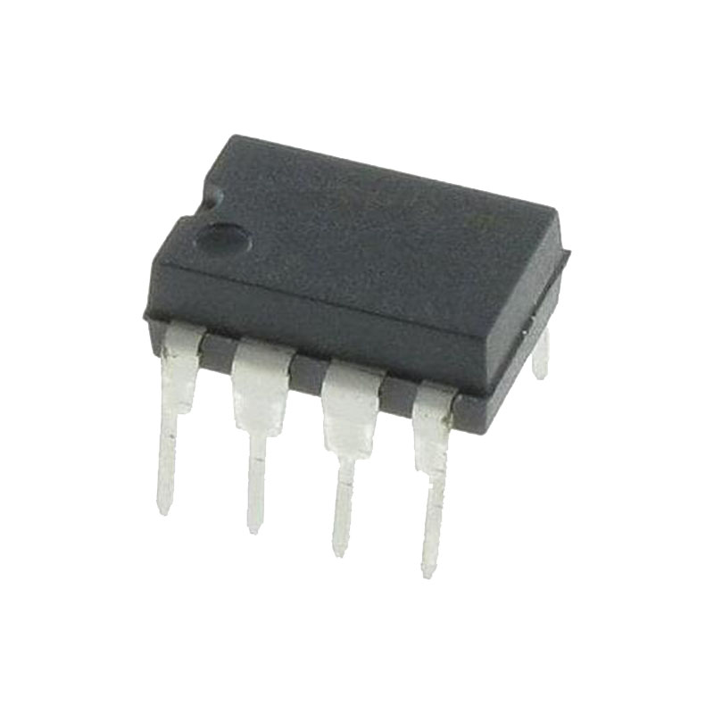
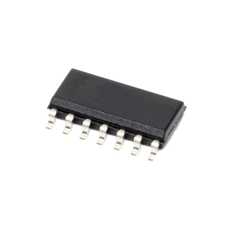
説明
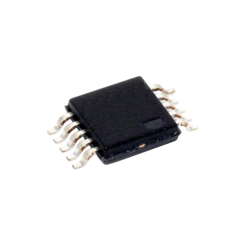
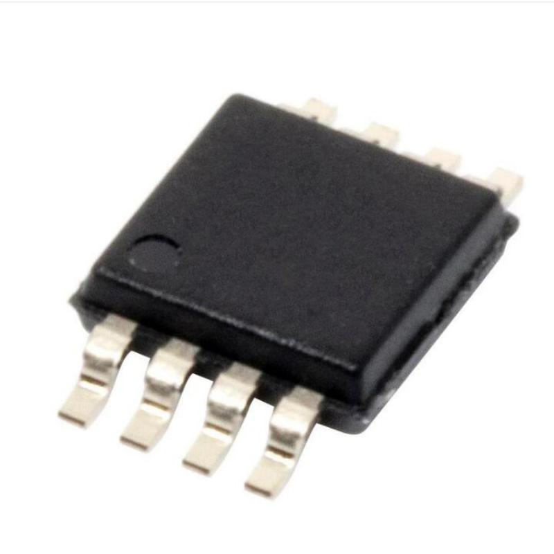
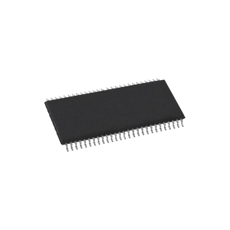
The LT1715 is an UltraFast dual comparator optimized for low voltage operation. Separate supplies allow independent analog input ranges and output logic levels with no loss of performance. The input voltage range extends from 100mV below VEE to 1.2V below VCC. Internal hysteresis makes the LT1715 easy to use even with slow moving input signals. The rail-to-rail outputs directly interface toTTL and CMOS. The symmetric output drive results in similar rise and fall times that can be harnessed for analog applications or for easy translation to other single supply logic levels. The LT1715 is available in the 10-pin MSOP package. The pinout of the LT1715 minimizes parasitic effects by placing the most sensitive inputs away from the outputs, shielded by the power rails.
特徴
UltraFast: 4ns at 20mV Overdriven
150MHz Toggle Frequency
Separate Input and Output Power Supplies
Low Power: 4.6mA per Comparator at 3V
Pinout Optimized for High Speed Use
Output Optimized for 3V and 5V Supplies
TTL/CMOS Compatible Rail-to-Rail Output
Input Voltage Range Extends 100mV Below Negative Rail
Internal Hysteresis with Specifi ed Limits
Specifi ed for –40°C to 125°C Temperature Range
Available in the 10-pin MSOP Package
アプリケーション
High Speed Differential Line Receivers
レベル翻訳者
Window Comparators
Crystal Oscillator Circuits
Threshold Detectors/Discriminators
High Speed Sampling Circuits
Delay Lines
アプリケーション情報
Power Supply Confi gurations
The LT1715 has separate supply pins for the input and output stages that allow fl exible operation, accommodating separate voltage ranges for the analog input and the output logic. Of course, a single 3V/5V supply may be used by tying +VS and VCC together as well as GND and VEE. The minimum voltage requirement can be simply stated as both the output and the input stages need at least 2.7V and the VEE pin must be equal to or less than ground.
Although the ground pin need not be tied to system ground, most applications will use it that way. The fi nal one is uncommon, but it will work and may be useful as a level translator; the input stage is run from –5.2V and ground while the output stage is run from 3V and ground. In this case the common mode input voltage range does not include ground, so it may be helpful to tie VCC to 3V. Conversely, VCC may also be tied below ground, as long as the above rules are not violated
Input Voltage Considerations
The LT1715 is specified for a common mode range of –100mV to 3.8V when used with a single 5V supply. A more general consideration is that the common mode range is 100mV below VEE to 1.2V below VCC. The criterion for this common mode limit is that the output still responds correctly to a small differential input signal. If one input is within the common mode limit, the other input signal can go outside the common mode limits, up to the absolute maximum limits, and the output will retain the correct polarity. When either input signal falls below the negative common mode limit, the internal PN diode formed with the substrate can turn on, resulting in signifi cant current fl ow through the die. An external Schottky clamp diode between the input and the negative rail can speed uprecovery from negative overdrive by preventing the substrate diode from turning on. When both input signals are below the negative common mode limit, phase reversal protection circuitry prevents false output inversion to at least –400mV common mode. However, the offset and hysteresis in this mode will increase dramatically, to as much as 15mV each. The input bias currents will also increase. When one input signal goes above the common mode range without exceeding a diode drop above the input supply rail, the input stage will remain biased and the comparator will maintain correct output polarity. Above this voltage, the input stage current source will saturate completely and the ESD protection diode will forward conduct. Once the aberrant input falls back into the common mode range, the comparator will respond correctly to valid input signals within less than 10ns.

