説明
LT3042は、ノイズに敏感なRFアプリケーションの電源用に、LTCの超低ノイズ、超高PSRRアーキテクチャを採用した高性能低ドロップアウト・リニア・レギュレータです。LT3042は、高精度電流リファレンスに高性能電圧バッファが続くように設計されており、ノイズをさらに低減し、出力電流を増加させ、PCB上の熱を拡散させるために、容易に並列化することができます。
このデバイスは、典型的な350mVのドロップアウト電圧で200mAを供給する。動作時の静止電流は公称2mAで、シャットダウン時には<<1μAまで低下します。ユニティゲイン動作を維持しながら、LT3042の広い出力電圧範囲(0V~15V)は、プログラムされた出力電圧とは無関係に、実質的に一定の出力ノイズ、PSRR、帯域幅、負荷レギュレーションを提供します。さらに、このレギュレータは、プログラム可能な電流制限、高速スタートアップ機能、出力電圧レギュレーションを示すプログラム可能なパワーグッドを備えています。
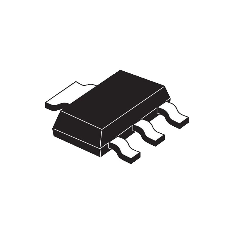
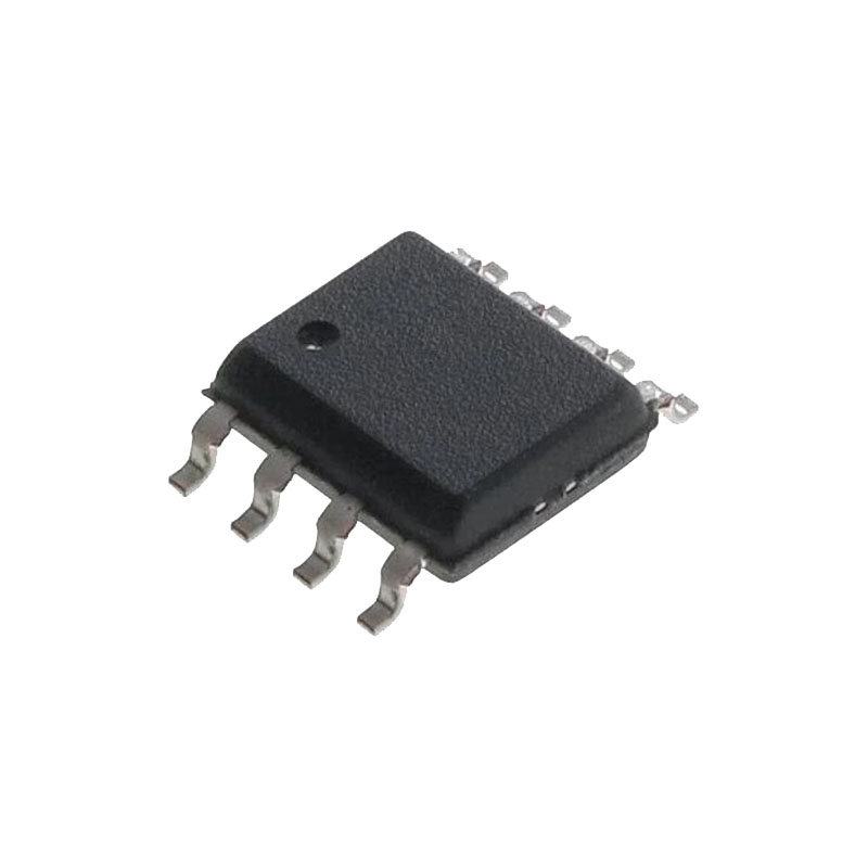
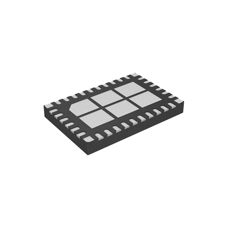
LT3042は、最小4.7μFのセラミック出力コンデンサで安定しています。内蔵保護機能には、逆バッテリ保護、逆電流保護、フォールドバック付き内部電流制限、ヒステリシス付き温度制限があります。LT3042は、熱的に強化された10リードMSOPおよび3mm×3mm DFNパッケージで提供されます。
特徴
超低RMSノイズ:0.8μVRMS(10Hz~100kHz)
超低スポットノイズ:10kHzで2nV/√Hz
超高PSRR:1MHzで79dB
出力電流:200mA
広い入力電圧範囲:1.8V〜20V
シングル・コンデンサーでノイズとPSRRを改善
100μA SET端子電流:±1% 初期精度
単一抵抗プログラム出力電圧
高帯域幅:1MHz
プログラマブル電流制限
低入出力電圧:350mV
出力電圧範囲0V〜15V
プログラマブル・パワー・グッド
迅速な立ち上げ能力
精密イネーブル/UVLO
低ノイズと大電流を実現するパラレル方式
フォールドバック付き内部電流制限
最小出力コンデンサ:4.7μFセラミック
逆バッテリーおよび逆電流保護
10ピンMSOPおよび3mm×3mm DFNパッケージ
自動車用AEC-Q100認定
アプリケーション
RF電源PLL、VCO、ミキサー、LNA
超低ノイズ計測器
高速/高精度データ・コンバータ
医療用途イメージング、診断
精密電源
スイッチング電源用ポストレギュレータ
アプリケーション情報
LT3042は、LTCの超低ノイズ(10kHzで2nV/√Hz)および超高PSRR(1MHzで79dB)アーキテクチャを特長とする高性能低ドロップアウト・リニア・レギュレータで、ノイズに敏感なアプリケーションに電源を供給します。LT3042は、高精度電流源の後に高性能のレールツーレール電圧バッファが続くように設計されており、ノイズをさらに低減し、出力電流を増加させ、PCB上の熱を分散させるために、容易に並列化することができます。このデバイスはさらに、プログラマブル電流制限、高速スタートアップ機能、プログラマブル・パワー・グッドを備えています。LT3042は使いやすく、高性能レギュレータに期待されるすべての保護機能を内蔵しています。短絡保護、安全動作領域保護、逆バッテリ保護、逆電流保護、ヒステリシス付きサーマルシャットダウンが含まれます。
プロテクション機能
LT3042は、バッテリ駆動アプリケーション向けにいくつかの保護機能を内蔵しています。高精度電流制限と熱過負荷保護は、デバイスの出力における過負荷や故障状態から LT3042 を保護します。通常動作では、ジャンクション温度が 125°C(E-, I グレード)または 150°C(H-, MP グレード)を超えないようにしてください。
LT3042の低ノイズエラーアンプを保護するため、SET-OUTS保護クランプはSET-OUTS間の最大電圧を制限し、クランプを介した最大DC電流は20mAである。そのため、SET を電圧源でアクティブに駆動するアプリケーションでは、電圧源の電流を 20mA 以下に制限する必要があります。さらに、過渡故障状態でこれらのクランプを流れる過渡電流を制限するために、SET ピンのコンデンサ(CSET)の最大値を 22μF に制限する。
LT3042は逆入力保護も内蔵しており、INピンは入力電流を流すことなく、またOUTピンに負電圧を発生させることなく、最大-20Vの逆電圧に耐えます。このレギュレータは、逆接続されたバッテリに対して、それ自身と負荷の両方を保護します。
バックアップ・バッテリーが必要な回路では、いくつかの異なる入出力状態が起こり得る。入力がGNDにプルされるか、中間電圧にプルされるか、またはオープン回路のまま、出力電圧が保持されることがあります。これら全ての場合において、逆電流保護回路が出力から入力への電流の流れを防止する。それにもかかわらず、OUTS-to-SETクランプにより、SETピンがフローティングでない限り、電流はSETピン抵抗を通してGNDに流れ、出力オーバーシュート回復回路を通してGNDに最大15mA流れる可能性がある。この出力オーバーシュート回復回路を流れる電流は、OUTSピンとSETピンの間にショットキーダイオードを配置し、そのアノードをOUTSピンとすることで大幅に減少させることができる。