説明
The LT3093 is a high performance low dropout negative linear regulator featuring ADI’s ultralow noise and ultrahigh PSRR architecture for powering noise sensitive applications. The device can be easily paralleled to further reduce noise, increase output current and spread heat on a PCB.
The LT3093 supplies 200mA at a typical 190mV dropout voltage. Operating quiescent current is nominally 2.35mA and drops to 3µA in shutdown. The device’s wide output voltage range (0V to –19.5V) error amplifier operates in unity-gain and provides virtually constant output noise, PSRR, bandwidth, and load regulation independent of the programmed output voltage. Additional features are a bipolar enable pin, programmable current limit, fast startup capability and programmable power good to indicate output voltage regulation. The regulator incorporates a tracking function to control an upstream supply to maintain a constant voltage across the LT3093 to minimize power dissipation and optimize PSRR.
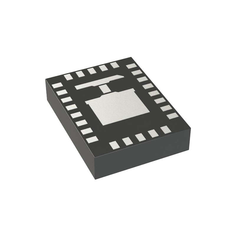
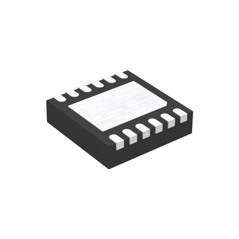
The LT3093 is stable with a minimum 4.7µF ceramic output capacitor. Built-in protection includes internal current limit with foldback and thermal limit with hysteresis. The LT3093 is available in thermally enhanced 12-Lead MSOP and 3mm × 3mm DFN Packages.
特徴
Ultralow RMS Noise: 0.8µVRMS (10Hz to 100kHz)
Ultralow Spot Noise: 2.2nV/√Hz at 10kHz
Ultrahigh PSRR: 73dB at 1MHz
出力電流:200mA
Wide Input Voltage Range: –1.8V to –20V
シングル・コンデンサーでノイズとPSRRを改善
100µA SET Pin Current: ±1% Initial Accuracy
単一抵抗プログラム出力電圧
プログラマブル電流制限
Low Dropout Voltage: 190mV
Output Voltage Range: 0V to –19.5V
Programmable Power Good and Fast Start-Up
Bipolar Precision Enable/UVLO Pin
VIOC Pin Controls Upstream Regulator to Minimize Power Dissipation and Optimize PSRR
Minimum Output Capacitor: 4.7µF Ceramic
12-Lead MSOP and 3mm × 3mm DFN Packages
アプリケーション
RF and Precision Power Supplies
超低ノイズ計測器
高速/高精度データ・コンバータ
Medical Applications: Diagnostics and Imaging
スイッチング電源用ポストレギュレータ
アプリケーション情報
The LT3093 is a high performance low dropout negative linear regulator featuring ADI’s ultralow noise (2.2nV/√Hz at 10kHz) and ultrahigh PSRR (73dB at 1MHz) architecture for powering noise sensitive applications. Designed as a precision current reference followed by a high performance rail-to-rail voltage buffer, the LT3093 can be easily paralleled to further reduce noise, increase output current and spread heat on the PCB. The device additionally features programmable current limit, fast start-up capability and programmable power good.
The LT3093 is easy to use and incorporates all of the protection features expected in high performance regulators. Included are short-circuit protection, safe operating area protection, and thermal shutdown with hysteresis.
Output Voltage
The LT3093 incorporates a precision 100µA current reference flowing into the SET pin, which also ties to the error amplifier’s inverting input.That connecting a resistor from SET to ground generates a reference voltage for the error amplifier. This reference voltage is simply the product of the SET pin current and the SET pin resistor. The error amplifier’s unity-gain configuration produces a low impedance version of this voltage on its noninverting input, i.e. the OUTS pin, which is externally tied to the OUT pin.
The LT3093’s rail-to-rail error amplifier and current reference architecture allows for a wide output voltage range from 0V (using a 0Ω resistor) to VIN minus dropout. An NPN-based input pair is active for a 0V to –0.8V output and a PNP-based input pair is active for output voltages beyond –1.5V, with a smooth transition between the two input pairs from –0.8V to –1.5V output. The PNP-based input pair offers the best overall performance; refer to the Electrical Characteristics table for details on offset voltage, SET pin current, output noise and PSRR variation depending on the output voltage and corresponding active input pair(s).