説明
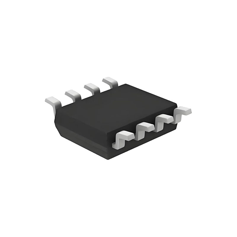
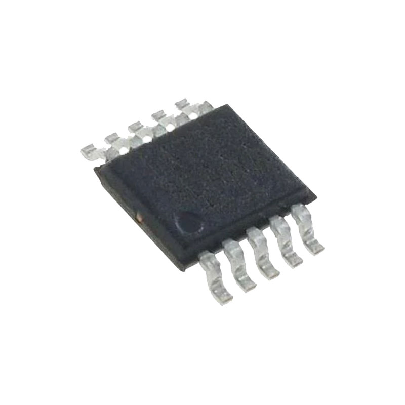
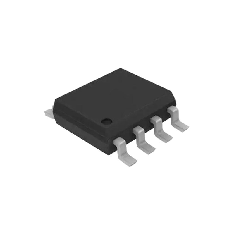
The LTC1864 are 16-bit A/D converters that are offered in MSOP and SO-8 packages and operate on a single 5V supply. At 250ksps, the supply current is only 850μA. The supply current drops at lower speeds because the LTC1864/LTC1865 automatically power down between conversions. These 16-bit switched capacitor successive approximation ADCs include sample-andholds. The LTC1864 has a differential analog input with an adjustable reference pin. The LTC1865 offers a softwareselectable 2-channel MUX and an adjustable reference pin on the MSOP version.
The 3-wire, serial I/O, small MSOP or SO-8 package and extremely high sample rate-to-power ratio make these ADCs ideal choices for compact, low power, high speed
systems. These ADCs can be used in ratiometric applications or with external references. The high impedance analog inputs and the ability to operate with reduced spans down to 1V full scale, allow direct connection to signal sources in many applications, eliminating the need for external gain stages.
特徴
16-Bit 250ksps ADCs in MSOP Package
Single 5V Supply
Low Supply Current: 850μA (Typ)
Auto Shutdown Reduces Supply Current to 2μA at 1ksps
True Differential Inputs
1-Channel (LTC1864)Versions
SPI/MICROWIRE™ Compatible Serial I/O
Guaranteed Operation to +125°C (MSOP Package)
アプリケーション
High Speed Data Acquisition
Portable or Compact Instrumentation
Low Power Battery-Operated Instrumentation
Isolated and/or Remote Data Acquisition
アプリケーション情報
Operating Sequence
The LTC1864 conversion cycle begins with the rising edge of CONV. After a period equal to tCONV, the conversion is finished. If CONV is left high after this time, the LTC1864 goes into sleep mode drawing only leakage current. On the falling edge of CONV, the LTC1864 goes into sample mode and SDO is enabled. SCK synchronizes the data transfer with each bit being transmitted from SDO on the falling SCK edge. The receiving system should capture the data from SDO on therising edge of SCK. After completing the data transfer, if further SCK clocks are applied with CONV low, SDO will output zeros indefinitely.
Analog Inputs
The LTC1864 has a unipolar differential analog input. The converter will measure the voltage between the “IN+” and “IN–” inputs. A zero code will occur when IN+ minus IN– equals zero. Full scale occurs when IN+ minus IN– equals VREF minus 1LSB. Both the “IN+” and “IN–” inputs are sampled at the same time, so common mode noise on the inputs is rejected by the ADC. If “IN–” is grounded and VREF is tied to VCC, a rail-to-rail input span will result on “IN+” .
Reference Input
The voltage on the reference input of the LTC1864 defi nes
the full-scale range of the A/D converter. The LTC1864 can
operate with reference voltages from VCC to 1V.
Reference Input
The voltage on the reference input of the LTC1864 defines the full-scale range of the A/D converter. The LTC1864 can operate with reference voltages from VCC to 1V.
Grounding
The LTC1864 should be used with an analog ground plane and single point grounding techniques. Do not use wire wrapping techniques to breadboard and evaluate the device. To achieve the optimum performance, use a printed circuit board. The ground pins should be tied directly to the analog ground plane with minimum lead length.
Bypassing
For good performance, the VCC and VREF pins must be free of noise and ripple. Any changes in the VCC/VREF voltage with respect to ground during the conversion cycle can induce errors or noise in the output code. Bypass the VCC and VREF pins directly to the analog ground plane with a minimum of 1μF tantalum. Keep the bypass capacitor leads as short as possible.
Analog Inputs
Because of the capacitive redistribution A/D conversion techniques used, the analog inputs of the LTC1864 have capacitive switching input current spikes. These current spikes settle quickly and do not cause a problem if source resistances are less than 200Ω or high speed op amps are used (e.g., the LT®1211, LT1469, LT1807, LT1810, LT1630, LT1226 or LT1215). But if large source resistances are used, or if slow settling op amps drive the inputs, take care to ensure the transients caused by the current spikes settle completely before the conversion begins.

