説明
LTM4628は完全なデュアル8A出力スイッチングモードDC/DC電源で、シングル2相16A出力に簡単に構成できます。パッケージには、スイッチングコントローラ、パワーFET、インダクタ、およびすべてのサポート部品が含まれています。入力電圧範囲4.5V~26.5Vで動作するLTM4628は、出力電圧範囲0.6V~5.5Vの2つの出力をそれぞれサポートし、1つの外部抵抗で設定できます。高効率設計により、各出力に8Aの連続電流を供給します。必要な入力および出力コンデンサはわずかです。
The device supports frequency synchronization, multiphase operation, Burst Mode operation and output voltage tracking for supply rail sequencing. It has an onboard temperature diode for device temperature monitoring. High switching frequency and a current mode architec
ture enable a very fast transient response to line and load changes without sacrificing stability.
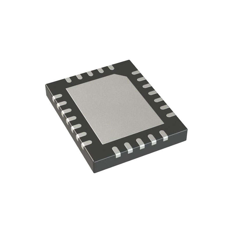
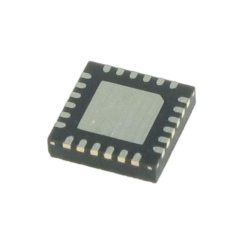
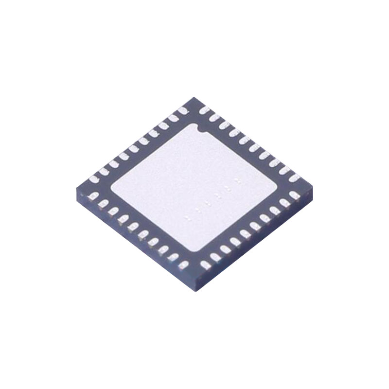
障害保護機能には、過電圧および過電流保護が含まれます。このパワーモジュールは、省スペースで熱対策が施された15mm×15mm×4.32mmのLGAおよび15mm×15mm×4.92mmのBGAパッケージで提供されます。LTM4628は、SnPb(BGA)またはRoHS準拠の端子仕上げで提供されます。
特徴
完全な独立型デュアル電源
シングル16Aまたはデュアル8A出力
広い入力電圧範囲:4.5V〜26.5V
出力電圧範囲0.6V〜5.5V
±1.5% DC出力総合誤差
差動リモートセンスアンプ
電流モード制御/高速過渡応答
調整可能なスイッチング周波数
過電流フォールドバック保護
複数のLTM4628による多相並列電流共有
周波数同期
内部温度検知ダイオード出力
選択可能なバースト・モード®動作
ソフトスタート/電圧トラッキング
出力過電圧保護
小型面実装フットプリント、薄型
15mm×15mm×4.32mmのLGAおよび
15mm × 15mm × 4.92mm BGAパッケージ
アプリケーション
通信・ネットワーク機器
ストレージとATCAカード
産業機器
アプリケーション情報
The typical LTM4628 application circuit is shown in Figure 28. External component selection is primarily determined by the maximum load current and output voltage. See Table 4 for specific external capacitor requirements for particular applications.VIN to VOUT Step-Down Ratios
与えられた入力電圧に対して達成できる最大 VIN および VOUT 降圧比には制限があります。LTM4628の各出力は98%のデューティ・サイクルが可能ですが、VINからVOUTの最小ドロップアウトは負荷電流の関数として示され、トップ側スイッチの高デューティ・サイクルに関連する出力電流能力が制限されます。最小オン時間tON(MIN)は、tON(MIN)<D/fSW(Dはデューティ・サイクル、fSWはスイッチング周波数)という事実により、ある周波数で動作しながら指定されたデューティ・サイクルで動作する際のもう1つの考慮事項である。
For parallel operation of multiple channels, the same feedback setting resistor can be used for the parallel design. This is done by connecting the VOUTS1 to the output as shown in Figure 2, thus tying one of the internal 60.4k resistors to the output. All of the VFB pins tie together with
one programming resistor as shown in Figure 2. In parallel operation, the VFB pins have an IFB current of 20nA maximum each channel. To reduce output voltage error due to this current, an additional VOUTS pin can be tied to VOUT, and an additional RFB resistor can be used to lower the total Thevenin’s equivalent resistance seen by this current. For example in Figure 2, the total
Thevenin’s equivalent resistance of the VFB pin is (60.4k // RFB), which is 30.2k where RFB is equal to 60.4k for a 1.2V output. Four phases connected in parallel equates to a worse case feedback current of 4•IFB equals 80nA maximum. The voltage error is 80nA•30.2k = 2.4mV. If
VOUTS2 is connected as shown in Figure 2 to VOUT, and another 60.4k resistor is connected from VFB2 to ground, then the voltage error is reduced to 1.2mV. If the voltage error is acceptable then no additional connections are necessary. The onboard 60.4k resistor is 0.5% accurate
and the VFB resistor can be chosen by the user to be as accurate as needed.
All COMP pins are tied together for current sharing between the phases. The TRACK pins can be tied together and a single soft-start capacitor can be used to softstart the regulator. The soft-start equation will need to have the soft-start current parameter increased by the number of paralleled channels. See the Output Voltage Tracking section.