GENERAL DESCRIPTION
The AD5241/AD52421 provide a single-/dual-channel, 256-position, digitally controlled variable resistor (VR) device. These devices perform the same electronic adjustment function as a potentiometer, trimmer, or variable resistor. Each VR offers a completely programmable value of resistance between the A terminal and the wiper, or the B terminal and the wiper. For the AD5242, the fixed A-to-B terminal resistance of 10 kΩ, 100 kΩ, or 1 MΩ has a 1% channel-to-channel matching tolerance. The nominal temperature coefficient of both parts is 30 ppm/°C.
Wiper position programming defaults to midscale at system power on. When powered, the VR wiper position is programmed by an I2C-compatible, 2-wire serial data interface. Both parts have two extra programmable logic outputs available that enable users to drive digital loads, logic gates, LED drivers, and analog switches in their system.
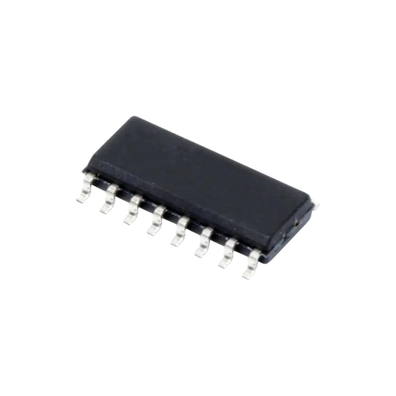
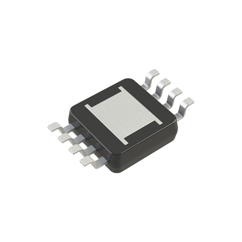
The AD5241/AD5242 are available in surface-mount, 14-lead SOIC and 16-lead SOIC packages and, for ultracompact solutions, 14-lead TSSOP and 16-lead TSSOP packages. All parts are guaranteed to operate over the extended temperature range of −40°C to +105°C.
FEATURES
256 positions
10 kΩ, 100 kΩ, 1 MΩ
Low temperature coefficient: 30 ppm/°C
Internal power on midscale preset
Single-supply 2.7 V to 5.5 V or dual-supply ±2.7 V for ac or bipolar operation
I2C-compatible interface with readback capability
Extra programmable logic outputs
Self contained shutdown feature
Extended temperature range: −40°C to +105°C
APPLICATIONS
Multimedia, video, and audio
Communications
Mechanical potentiometer replacement
Instrumentation: gain, offset adjustment
Programmable voltage-to-current conversion
Line impedance matching
THEORY OF OPERATION
The AD5241/AD5242 provide a single-/dual-channel, 256-position digitally controlled variable resistor (VR) device. The terms VR, RDAC, and programmable resistor are commonly used interchangeably to refer to digital potentiometer.
To program the VR settings, refer to the Digital Interface section. Both parts have an internal power-on preset that places the wiper in midscale during power-on that simplifies the fault condition recovery at power-up. In addition, the shutdown pin (SHDN) of AD5241/ AD5242 places the RDAC in an almost zero power consumption state where Terminal A is open circuited and Wiper W is connected to Terminal B, resulting in only leakage current being consumed in the VR structure. During shutdown, the VR latch contents are maintained when the RDAC is inactive. When the part returns from shutdown, the stored VR setting is applied to the RDAC.
PROGRAMMING THE VARIABLE RESISTOR
Rheostat Operation
The nominal resistance of the RDAC between Terminal A and Terminal B is available in 10 kΩ, 100 kΩ, and 1 MΩ. The final two or three digits of the part number determine the nominal resistance value, for example, 10 kΩ = 10, 100 kΩ = 100, and 1 MΩ = 1 M. The nominal resistance (RAB) of the VR has 256 contact points accessed by the wiper terminal, plus the B terminal contact. The 8-bit data in the RDAC latch is decoded to select one of the 256 possible settings. Assume a 10 kΩ part is used; the first connection of the wiper starts at the B terminal for Data 0x00. Because there is a 60 Ω wiper contact resistance, such connection yields a minimum of 60 Ω resistance between Terminal W and Terminal B. The second connection is the first tap point that corresponds to 99 Ω (RWB = RAB/256 + RW = 39 + 60) for Data 0x01. The third connection is the next tap point representing 138 Ω (39 × 2 + 60) for Data 0x02, and so on. Each LSB data value increase moves the wiper up the resistor ladder until the last tap point is reached at 10,021 Ω [RAB – 1 LSB + RW].
Note that in the zero-scale condition, a finite wiper resistance of 60 Ω is present. Care should be taken to limit the current flow between W and B in this state to a maximum current of no more than 20 mA. Otherwise, degradation or possible destruction of the internal switch contact can occur.
Similar to the mechanical potentiometer, the resistance of the RDAC between Wiper W and Terminal A also produces a digitally controlled resistance, RWA. When these terminals are used, Terminal B can be opened or tied to the wiper terminal. The minimum RWA resistance is for Data 0xFF and increases as the data loaded in the latch decreases in value.
The typical distribution of the nominal resistance RAB from channel to channel matches within ±1% for AD5242. Device-to-device matching is process lot dependent, and it is possible to have ±30% variation. Because the resistance element is processed in thin film technology, the change in RAB with temperature has no more than a 30 ppm/°C temperature coefficient.

