GENERAL DESCRIPTION
The AD5360/AD5361 contain sixteen, 16-/14-bit DACs in a single 52-lead LQFP or 56-lead LFCSP package. They provide buffered voltage outputs with a span four times the reference voltage. The gain and offset of each DAC can be independently trimmed to remove errors. For even greater flexibility, the device is divided into two groups of eight DACs, and the output range of each group can be independently adjusted by an offset DAC.
The AD5360/AD5361 offer guaranteed operation over a wide supply range with VSS from −4.5 V to −16.5 V and VDD from +8 V to +16.5 V. The output amplifier headroom requirement is 1.4 V.
The AD5360/AD5361 have a high speed 4-wire serial interface, which is compatible with SPI, QSPI™, MICROWIRE™, and DSP interface standards and can handle clock speeds of up to 50 MHz. All the outputs can be updated simultaneously by taking the LDAC input low. Each channel has a programmable gain register and an offset adjust register.
Each DAC output is amplified and buffered on-chip with respect to an external SIGGNDx input. The DAC outputs can also be switched to SIGGNDx via the CLR pin.
FEATURES
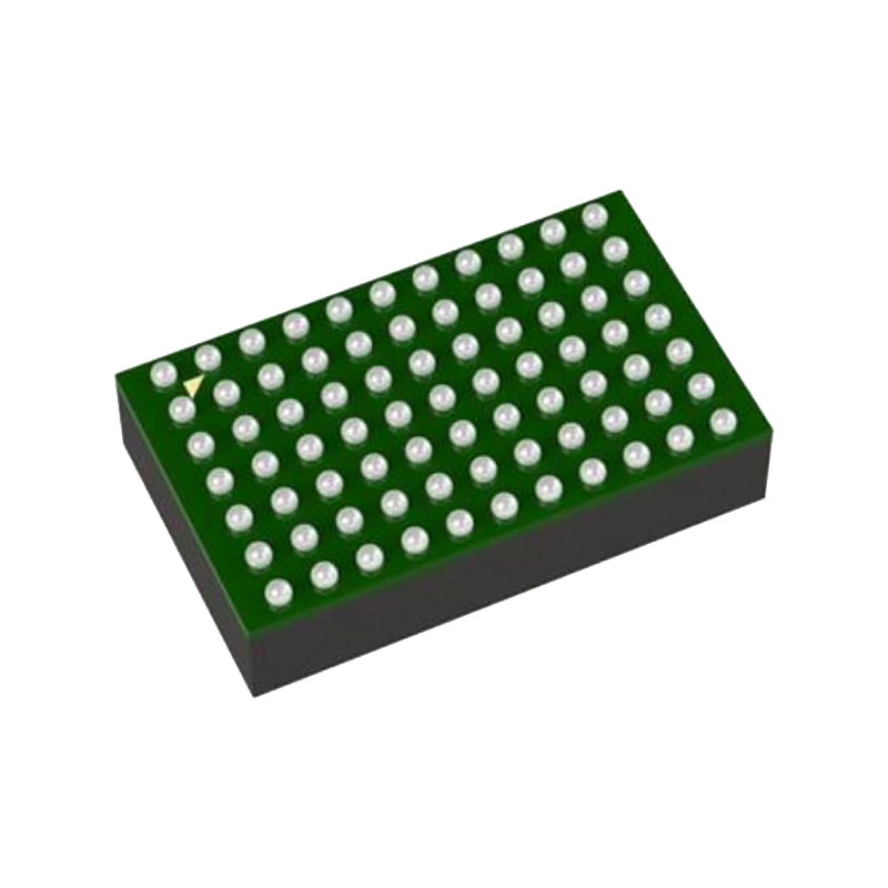
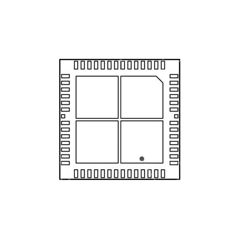
16-channel DAC in 52-lead LQFP and 56-lead LFCSP packages
Guaranteed monotonic to 16/14 bits
Nominal output voltage range of −10 V to +10 V
Multiple output spans available
Temperature monitoring function
Channel monitoring multiplexer
GPIO function
System calibration function allowing user-programmable offset and gain
Channel grouping and addressing features
Data error checking feature
SPI-compatible serial interface
2.5 V to 5.5 V digital interface
Digital reset (RESET)
Clear function to user-defined SIGGNDx
Simultaneous update of DAC outputs
APPLICATIONS
Instrumentation
Industrial control systems
Level setting in automatic test equipment (ATE)
Variable optical attenuators (VOA)
Optical line cards
FUNCTIONAL
DESCRIPTION DAC ARCHITECTURE
The AD5360/AD5361 contain 16 DAC channels and 16 output amplifiers in a single package. The architecture of a single DAC channel consists of a 16-bit resistor-string DAC in the case of the AD5360 and a 14-bit DAC in the case of the AD5361, followed by an output buffer amplifier. The resistor-string section is simply a string of resistors, of equal value, from VREF0 or VREF1 to AGND. This type of architecture guarantees DAC monotonicity. The 16-/14-bit binary digital code loaded to the DAC register determines at which node on the string the voltage is tapped off before being fed into the output amplifier. The output amplifier multiplies the DAC output voltage by 4. The nominal output span is 12 V with a 3 V reference and 20 V with a 5 V reference.
CHANNEL GROUPS
The 16 DAC channels of the AD5360/AD5361 are arranged into two groups of eight channels. The eight DACs of Group 0 derive their reference voltage from VREF0. Group 1 derives its reference voltage from VREF1. Each group has its own signal ground pin.
A/B REGISTERS GAIN/OFFSET ADJUSTMENT
Each DAC channel has seven data registers. The actual DAC data word can be written to either the X1A or X1B input register, depending on the setting of the A/B bit in the control register. If the A/B bit is 0, data is written to the X1A register. If the A/B bit is 1, data is written to the X1B register. Note that this single bit is a global control and affects every DAC channel in the device. It is not possible to set up the device on a perchannel basis so that some writes are to the X1A register and some writes are to the X1B register.
Each DAC channel also has a gain register (M) and an offset (C) register, which allow trimming out of the gain and offset errors of the entire signal chain. Data from the X1A register is operated on by a digital multiplier and adder by the contents of the M and C registers. The calibrated DAC data is then stored in the X2A register. Similarly, data from the X1B register is operated on by the multiplier and adder and stored in the X2B register.
Although a multiplier and adder symbol are shown for each channel, there is only one multiplier and one adder in the device, which are shared among all channels. This has implications for the update speed when several channels are updated at once, as described in the Register Update Rates section.
Each time data is written to the X1A register, or to the M or C register with the A/B control bit set to 0, the X2A data is recalculated and the X2A register is automatically updated. Similarly, X2B is updated each time data is written to X1B, or to M or C with A/B set to 1. The X2A and X2B registers are not readable or directly writable by the user.
Data output from the X2A and X2B registers is routed to the final DAC register by a multiplexer. An 8-bit A/B select register associated with each group of eight DACs controls whether each individual DAC takes its data from the X2A or X2B register. If a bit in this register is 0, the DAC takes its data from the X2A register; if 1, the DAC takes its data from the X2B register (Bit 0 through Bit 7 control DAC 0 through DAC 7, respectively).
Note that because there are 16 bits in two registers, it is possible to set up, on a per-channel basis, whether each DAC takes its data from the X2A register or X2B register. A global command is also provided that sets all bits in the A/B select registers to 0 or to 1.
All DACs in the AD5360/AD5361 can be updated simultaneously by taking LDAC low, when each DAC register is updated from either its X2A or X2B register, depending on the setting of the A/B select registers. The DAC register is not readable or directly writable by the user.