GENERAL DESCRIPTION
The AD7606/AD7606-6/AD7606-4 are 16-bit, simultaneous sampling, analog-to-digital data acquisition systems (DAS) with eight, six, and four channels, respectively. Each part contains analog input clamp protection, a second-order antialiasing filter, a track-and-hold amplifier, a 16-bit charge redistribution successive approximation analog-to-digital converter (ADC), a flexible digital filter, a 2.5 V reference and reference buffer, and high speed serial and parallel interfaces.
The AD7606/AD7606-6/AD7606-4 operate from a single 5 V supply and can accommodate ±10 V and ±5 V true bipolar input signals while sampling at throughput rates up to 200 kSPS for all channels. The input clamp protection circuitry can tolerate voltages up to ±16.5 V. The AD7606 has 1 MΩ analog input impedance regardless of sampling frequency. The single supply operation, on-chip filtering, and high input impedance eliminate the need for driver op amps and external bipolar supplies. The AD7606/AD7606-6/ AD7606-4 antialiasing filter has a 3 dB cutoff frequency of 22 kHz and provides 40 dB antialias rejection when sampling at 200 kSPS. The flexible digital filter is pin driven, yields improvements in SNR, and reduces the 3 dB bandwidth.
FEATURES
8/6/4 simultaneously sampled inputs
True bipolar analog input ranges: ±10 V, ±5 V
Pin to pin compatible with the state-of-the-art AD7606B
Single 5 V analog supply and 2.3 V to 5 V VDRIVE
Fully integrated data acquisition solution
Analog input clamp protection
Input buffer with 1 MΩ analog input impedance
Second-order antialiasing analog filter
On-chip accurate reference and reference buffer
16-bit ADC with 200 kSPS on all channels
Oversampling capability with digital filter
Flexible parallel/serial interface
SPI/QSPI™/MICROWIRE™/DSP compatible
Performance
7 kV ESD rating on analog input channels
95.5 dB SNR, −107 dB THD
±0.5 LSB INL, ±0.5 LSB DNL
Low power: 100 mW
Standby mode: 25 mW
Temperature range: −40°C to +85°C
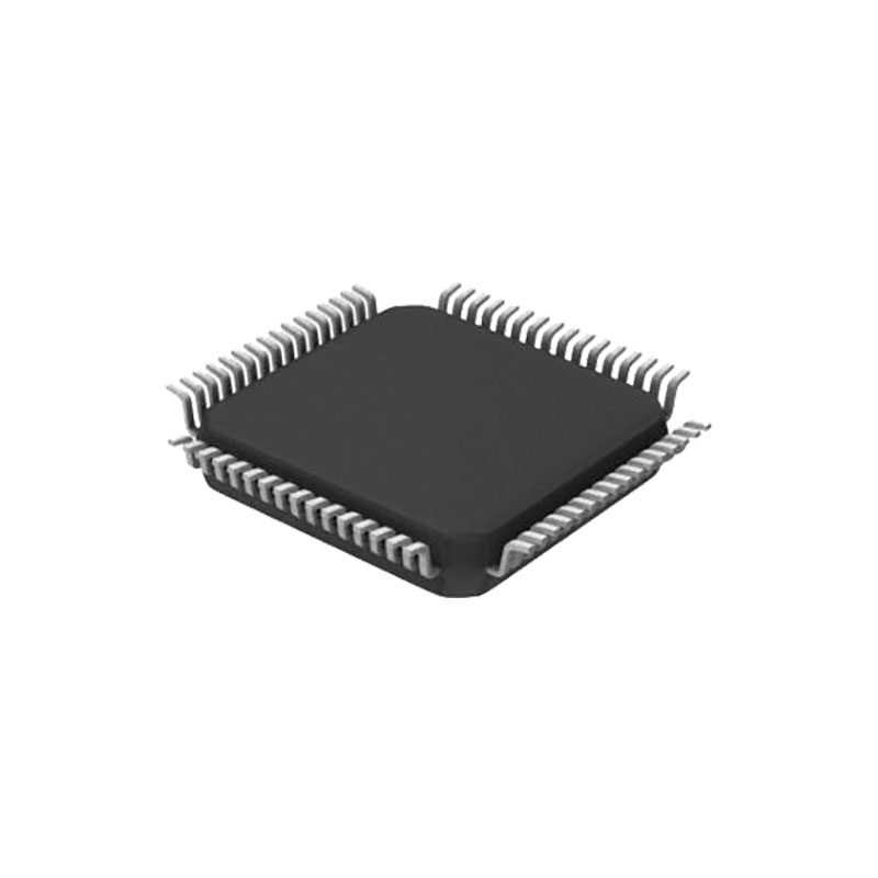
64-lead LQFP package
APPLICATIONS
Power-line monitoring and protection systems
Multiphase motor control
Instrumentation and control systems
Multiaxis positioning systems
Data acquisition systems (DAS)
THEORY OF OPERATION
CONVERTER DETAILS
The AD7606/AD7606-6/AD7606-4 are data acquisition systems that employ a high speed, low power, charge redistribution, successive approximation analog-to-digital converter (ADC) and allow the simultaneous sampling of eight/six/four analog input channels. The analog inputs on the AD7606/AD7606-6/AD7606-4 can accept true bipolar input signals. The RANGE pin is used to select either ±10 V or ±5 V as the input range. The AD7606/AD7606-6/AD7606-4 operate from a single 5 V supply.
The AD7606/AD7606-6/AD7606-4 contain input clamp protection, input signal scaling amplifiers, a second-order anti-aliasing filter, track-and-hold amplifiers, an on-chip reference, reference buffers, a high speed ADC, a digital filter, and high speed parallel and serial interfaces. Sampling on the AD7606/AD7606-6/AD7606-4 is controlled using the CONVST signals.
ANALOG INPUT
Analog Input Ranges
The AD7606/AD7606-6/AD7606-4 can handle true bipolar, singleended input voltages. The logic level on the RANGE pin determines the analog input range of all analog input channels. If this pin is tied to a logic high, the analog input range is ±10 V for all channels. If this pin is tied to a logic low, the analog input range is ±5 V for all channels. A logic change on this pin has an immediate effect on the analog input range; however, there is typically a settling time of approximately 80 μs, in addition to the normal acquisition time requirement. The recommended practice is to hardwire the RANGE pin according to the desired input range for the system signals.
During normal operation, the applied analog input voltage should remain within the analog input range selected via the RANGE pin. A RESET pulse must be applied after power up to ensure the analog input channels are configured for the range selected.
When in a power-down mode, it is recommended to tie the analog inputs to GND. Per the Analog Input Clamp Protection section, the overvoltage clamp protection is recommended for use in transient overvoltage conditions and should not remain active for extended periods. Stressing the analog inputs outside of the conditions mentioned here may degrade the bipolar zero code error and THD performance of the AD7606/AD7606-6/AD7606-4.

