GENERAL DESCRIPTION
The AD76901 is an 18-bit, successive approximation, analog-todigital converter (ADC) that operates from a single power supply, VDD. It contains a low power, high speed, 18-bit sampling ADC with no missing codes, an internal conversion clock, and a versatile serial interface port. On the CNV rising edge, it samples the voltage difference between the IN+ and IN− pins. The voltages on these pins swing in opposite phase between 0 V and REF. The reference voltage, REF, is applied externally and can be set up to the supply voltage. The power of the AD7690 scales linearly with the throughput. The SPI-compatible serial interface also features the ability, using the SDI input, to daisy-chain several ADCs on a single, 3-wire bus and provides an optional busy indicator. It is compatible with 1.8 V, 2.5 V, 3 V, or 5 V logic, using the separate VIO supply. The AD7690 is housed in a 10-lead MSOP or a 10-lead LFCSP with operation specified from −40°C to +85°C.
APPLICATIONS
Battery-powered equipment
Data acquisition
Seismic data acquisition systems
DVMs
Instrumentation
Medical instruments
FEATURES
18-bit resolution with no missing codes
Throughput: 400 kSPS
INL: ±0.75 LSB typical, ±1.5 LSB maximum (±6 ppm of FSR)
Dynamic range: 102 dB at 400 kSPS
Oversampled dynamic range: 125 dB at 1 kSPS
Noise-free code resolution: 20 bits at 1 kSPS
Effective resolution: 22.7 bits at 1 kSPS
SINAD: 101.5 dB at 1 kHz
THD: −125 dB at 1 kHz
True differential analog input range: ±VREF
0 V to VREF with VREF up to VDD on both inputs
No pipeline delay
Single-supply 5 V operation with
1.8 V/2.5 V/3 V/5 V logic interface
Proprietary serial interface
SPI/QSPI/MICROWIRE™/DSP compatible
Daisy-chain multiple ADCs and busy indicator
Power dissipation
4.25 μW at 100 SPS
4.25 mW at 100 kSPS
Standby current: 1 nA
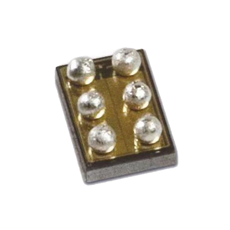
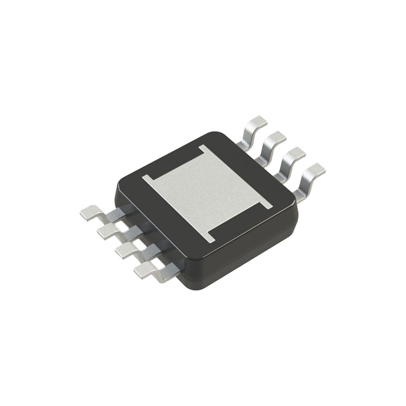
10-lead package: MSOP (MSOP-8 size) and
3 mm × 3 mm LFCSP (SOT-23 size)
Pin-for-pin compatible with LFCSP/MSOP PulSAR ADCs
CONVERTER OPERATION
The AD7690 is a successive approximation ADC based on a charge redistribution DAC.The capacitive DAC consists of two identical arrays of 18 binary-weighted capacitors, which are connected to the two comparator inputs.
During the acquisition phase, terminals of the array tied to the comparator’s input are connected to GND via SW+ and SW−. All independent switches are connected to the analog inputs. Thus, the capacitor arrays are used as sampling capacitors and acquire the analog signal on the IN+ and IN− inputs. When the acquisition phase is complete and the CNV input goes high, a conversion phase is initiated. When the conversion phase begins, SW+ and SW− are opened first. The two capacitor arrays are then disconnected from the inputs and connected to the GND input. Therefore, the differential voltage between the IN+ and IN− inputs captured at the end of the acquisition phase is applied to the comparator inputs, causing the comparator to become unbalanced. By switching each element of the capacitor array between GND and REF, the comparator input varies by binary-weighted voltage steps (VREF/2, VREF/4 … VREF/262,144).
The control logic toggles these switches, starting with the MSB, to bring the comparator back into a balanced condition. After the completion of this process, the part returns to the acquisition phase, and the control logic generates the ADC output code and a busy signal indicator.
Because the AD7690 has an on-board conversion clock, the serial clock, SCK, is not required for the conversion process.For more information, please refer to the specifications.