GENERAL DESCRIPTION
The AD8221 is a gain programmable, high performance instrumentation amplifier that delivers the industry’s highest CMRR over frequency in its class. The CMRR of instrumentation amplifiers on the market today falls off at 200 Hz. In contrast, the AD8221 maintains a minimum CMRR of 80 dB to 10 kHz for all grades at G = 1. High CMRR over frequency allows the AD8221 to reject wideband interference and line harmonics, greatly simplifying filter requirements. Possible applications include precision data acquisition, biomedical analysis, and aerospace instrumentation. Low voltage offset, low offset drift, low gain drift, high gain accuracy, and high CMRR make this part an excellent choice in applications that demand the best dc performance possible, such as bridge signal conditioning. Programmable gain affords the user design flexibility. A single resistor sets the gain from 1 to 1000. The AD8221 operates on
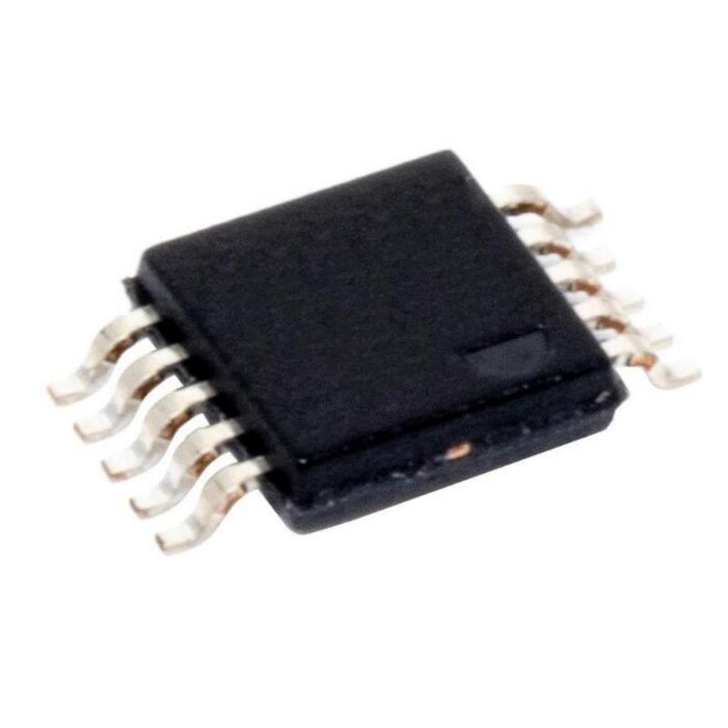
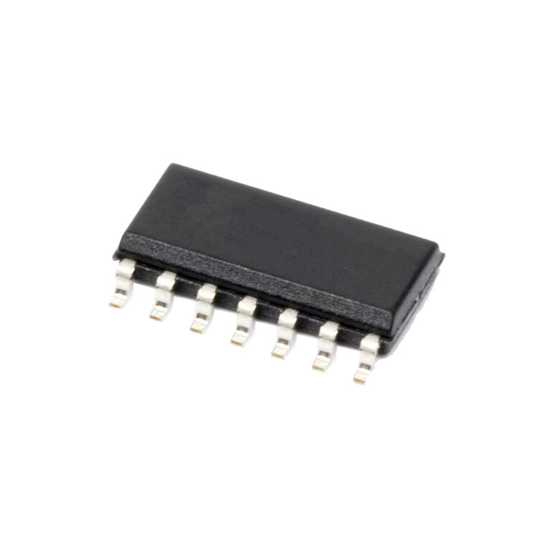
both single and dual supplies and is well suited for applications where ±10 V input voltages are encountered. The AD8221 is available in a low cost 8-lead SOIC and 8-lead MSOP, both of which offer the industry’s best performance. The MSOP requires half the board space of the SOIC, making it ideal for multichannel or space-constrained applications. Performance is specified over the entire industrial temperature range of −40°C to +85°C for all grades. Furthermore, the AD8221 is operational from −40°C to +125°C
FEATURES
Easy to use Available in space-saving MSOP
Gain set with 1 external resistor (gain range 1 to 1000)
Wide power supply range: ±2.3 V to ±18 V
Temperature range for specified performance: −40°C to +85°C
Operational up to 125°C
Excellent AC specifications
80 dB minimum CMRR to 10 kHz (G = 1)
825 kHz, –3 dB bandwidth (G = 1)
2 V/µs slew rate
Low noise
8 nV/√Hz, @ 1 kHz, maximum input voltage noise
0.25 µV p-p input noise (0.1 Hz to 10 Hz)
High accuracy dc performance (AD8221BR)
90 dB minimum CMRR (G = 1)
25 µV maximum input offset voltage
0.3 µV/°C maximum input offset drift
0.4 nA maximum input bias current
APPLICATIONS
Weigh scales
Industrial process controls
Bridge amplifiers
Precision data acquisition systems
Medical instrumentation
Strain gages
Transducer interfaces
THEORY OF OPERATION
The AD8221 is a monolithic instrumentation amplifier based on the classic 3-op amp topology. Input transistors Q1 and Q2 are biased at a fixed current so that any differential input signal forces the output voltages of A1 and A2 to change accordingly. A signal applied to the input creates a current through RG , R1, and R2, such that the outputs of A1 and A2 deliver the correct voltage. Topologically, Q1, A1, R1 and Q2, A2, R2 can be
viewed as precision current feedback amplifiers. The amplified differential and common-mode signals are applied to a difference amplifier that rejects the common-mode voltage but amplifies the differential voltage. The difference amplifier employs innovations that result in low output offset voltage as well as low output offset voltage drift. Laser-trimmed resistors allow for a highly accurate in-amp with gain error typically less than 20 ppm and CMRR that exceeds 90 dB (G = 1).
Because the input amplifiers employ a current feedback architecture, the gain-bandwidth product of the AD8221 increases with gain, resulting in a system that does not suffer from the expected bandwidth loss of voltage feedback architectures at higher gains. To maintain precision even at low input levels, special attention was given to the design and layout of the AD8221, resulting in an in-amp whose performance satisfies the most demanding applications.