GENERAL DESCRIPTION
This family of amplifiers has ultralow offset, drift, and bia scurrent. The AD8571/AD8572/AD8574 are single, dual, and quad amplifiers, respectively, featuring rail-to-rail input and output swings. All are guaranteed to operate from 2.7 V to 5 V single supply.
The AD8571/AD8572/AD8574 provide benefits previously found only in expensive auto-zeroing or chopper-stabilized amplifiers. Using Analog Devices, Inc., topology, these zero drift amplifiers combine low cost with high accuracy. (No external capacitors are required.) Using a spread-spectrum, auto-zero technique, the AD8571/AD8572/AD8574 eliminate the intermodulation effects from interaction of the chopping function with the signal frequency in ac applications.
With an offset voltage of only 1 μV and drift of 0.005 μV/°C, the AD8571/AD8572/AD8574 are perfectly suited for applications where error sources cannot be tolerated. Position and pressure sensors, medical equipment, and strain gage amplifiers benefit greatly from nearly zero drift over their operating temperature range. Many more systems require the rail-to-rail input and output swings provided by the AD8571/AD8572/AD8574.
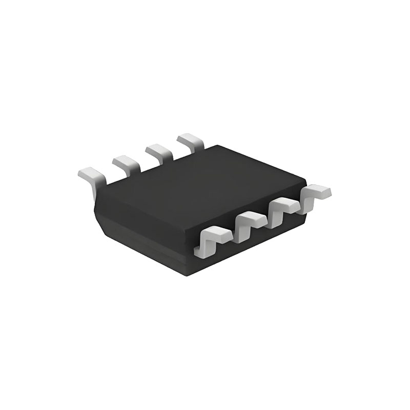
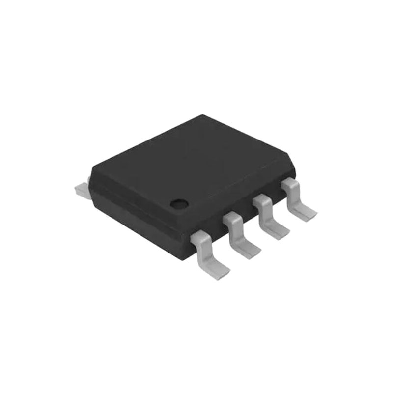
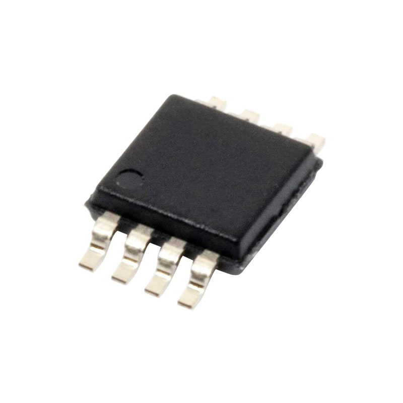
The AD8571/AD8572/AD8574 are specified for the extended industrial/ automotive temperature range (−40°C to +125°C). The AD8572 dual amplifier is available in 8-lead narrow SOIC and surface-mount TSSOP packages.
FEATURES
Low offset voltage: 1 μV
Input offset drift: 0.005 μV/°C
Rail-to-rail input and output swing
5 V/2.7 V single-supply operation
High gain: 145 dB typical
CMRR: 140 dB typical
PSRR: 130 dB typical
Ultralow input bias current: 10 pA typical
Low supply current: 750 μA per op amp
Overload recovery time: 50 μs
No external capacitors required
APPLICATIONS
Temperature sensors
Pressure sensors
Precision current sensing
Strain gage amplifiers
Medical instrumentation
Thermocouple amplifiers
FUNCTIONAL DESCRIPTION
The AD8571/AD8572/AD8574 are CMOS amplifiers that achieve their high degree of precision through random frequency auto-zero stabilization. The autocorrection topology allows the AD8571/AD8572/AD8574 to maintain its low offset voltage over a wide temperature range, and the randomized auto-zero clock eliminates any inter-modulation distortion (IMD) errors at the amplifier output.
The AD8571/AD8572/AD8574 can run from a single-supply voltage as low as 2.7 V. The extremely low offset voltage of 1 μV and no IMD products allow the amplifier to be easily configured for high gains without risk of excessive output voltage errors, which makes the AD8571/AD8572/AD8574 an ideal amplifier for applications requiring both dc precision and low distortion for ac signals. The extremely small temperature drift of 5 nV/°C ensures a minimum of offset voltage error over its −40°C to +125°C temperature range. These combined features make the AD8571/AD8572/AD8574 an excellent choice for a variety of sensitive measurement and automotive applications.
AMPLIFIER ARCHITECTURE
Each AD8571/AD8572/AD8574 op amp consists of two amplifiers: a main amplifier and a secondary amplifier that is used to correct the offset voltage of the main amplifier. Both consist of a rail-to-rail input stage, allowing the input common-mode voltage range to reach both supply rails. The input stage consists of an NMOS differential pair operating concurrently with a parallel PMOS differential pair. The outputs from the differential input stages are combined in another gain stage whose output is used to drive a rail-to-rail output stage.
The wide voltage swing of the amplifier is achieved by using two output transistors in a common-source configuration. The output voltage range is limited by the drain-to-source resistance of these transistors. As the amplifier is required to source or sink more output current, the voltage drop across these transistors increases due to their on resistance (RDS). Simply put, the output voltage does not swing as close to the rail under heavy output current conditions as it does with light output current. This is a characteristic of all rail-to-rail output amplifiers. Figure 12 and Figure 13 show how close the output voltage can get to the rails with a given output current. The output of the AD8571/ AD8572/AD8574 is short-circuit protected to approximately 50 mA of current.
The AD8571/AD8572/AD8574 amplifiers have exceptional gain, yielding greater than 120 dB of open-loop gain with a load of 2 kΩ. Because the output transistors are configured in a common-source configuration, the gain of the output stage, and thus the open-loop gain of the amplifier, is dependent on the load resistance. Open-loop gain decreases with smaller load resistances, which is another characteristic of rail-to-rail output amplifiers.

