GENERAL DESCRIPTION
The AD9642 is a 14-bit analog-to-digital converter (ADC) with sampling speeds of up to 250 MSPS. The AD9642 is designed to support communications applications, where low cost, small size, wide bandwidth, and versatility are desired.
The ADC core features a multistage, differential pipelined architecture with integrated output error correction logic. The ADC features wide bandwidth inputs that can support a variety of user-selectable input ranges. An integrated voltage reference eases design considerations. A duty cycle stabilizer (DCS) is provided to compensate for variations in the ADC clock duty cycle, allowing the converter to maintain excellent performance.
The ADC output data is routed directly to the external 14-bit LVDS output port.
Flexible power-down options allow significant power savings, when desired.
Programming for setup and control is accomplished using a 3-wire SPI-compatible serial interface.
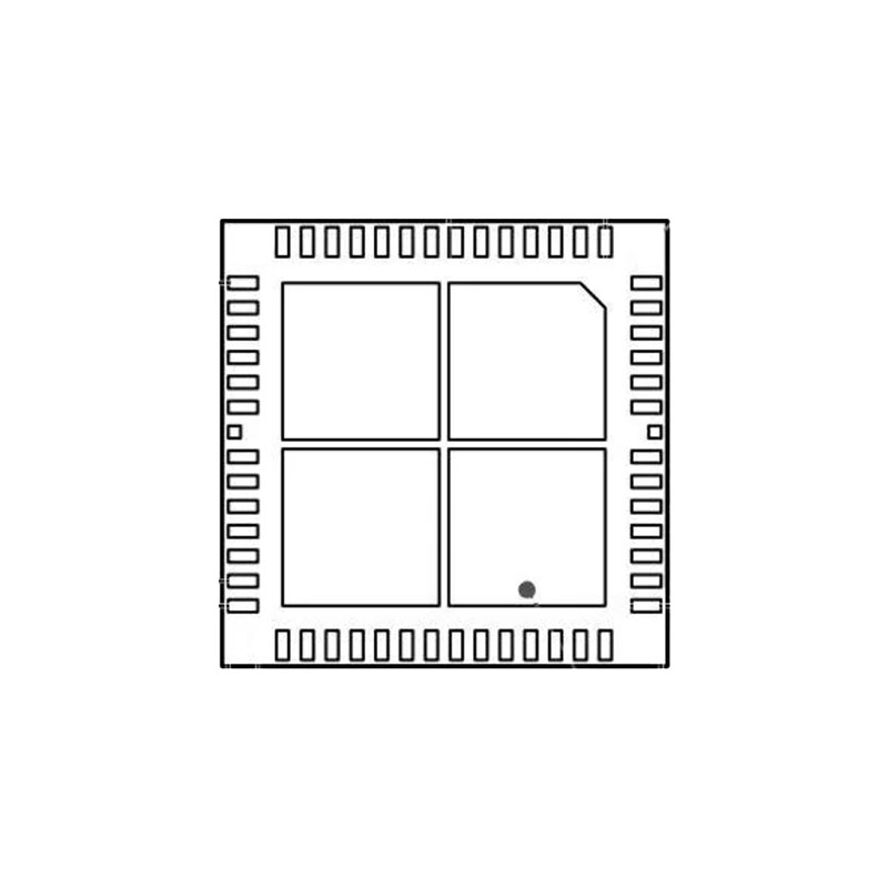
The AD9642 is available in a 32-lead LFCSP and is specified over the industrial temperature range of −40°C to +85°C. This product is protected by a U.S. patent.
APPLICATIONS
Communications
Diversity radio systems
Multimode digital receivers (3G)
TD-SCDMA, WiMAX, WCDMA, CDMA2000, GSM, EDGE, LTE
I/Q demodulation systems
Smart antenna systems
General-purpose software radios
Ultrasound equipment
Broadband data applications
FEATURES
SNR = 71.0 dBFS at 185 MHz AIN and 250 MSPS
SFDR = 83 dBc at 185 MHz AIN and 250 MSPS
−152.0 dBFS/Hz input noise at 200 MHz, −1 dBFS AIN, 250 MSPS
Total power consumption: 390 mW at 250 MSPS
1.8 V supply voltages
LVDS (ANSI-644 levels) outputs
Integer 1-to-8 input clock divider (625 MHz maximum input)
Sample rates of up to 250 MSPS
Internal ADC voltage reference
Flexible analog input range 1.4 V p-p to 2.0 V p-p (1.75 V p-p nominal)
ADC clock duty cycle stabilizer
Serial port control
Energy saving power-down modes
PRODUCT HIGHLIGHTS
Integrated 14-bit, 170 MSPS/210 MSPS/250 MSPS ADC.
Operation from a single 1.8 V supply and a separate digital output driver supply accommodating LVDS outputs.
Proprietary differential input maintains excellent SNR performance for input frequencies of up to 350 MHz.
3-pin, 1.8 V SPI port for register programming and readback.
Pin compatibility with the AD9634, allowing a simple migration from 14 bits to 12 bits, and with the AD6672.
THEORY OF OPERATION
The AD9642 can sample any fS/2 frequency segment from dc to 250 MHz using appropriate low-pass or band-pass filtering at the ADC inputs with little loss in ADC performance. Programming and control of the AD9642 are accomplished using a 3-pin, SPI-compatible serial interface.
ADC ARCHITECTURE
The AD9642 architecture consists of a front-end sample-andhold circuit, followed by a pipelined switched-capacitor ADC. The quantized outputs from each stage are combined into a final 14-bit result in the digital correction logic. The pipelined architecture permits the first stage to operate on a new input sample and the remaining stages to operate on the preceding samples. Sampling occurs on the rising edge of the clock.
The input stage of the AD9642 contains a differential sampling circuit that can be ac- or dc-coupled in differential or singleended modes. The output staging block aligns the data, corrects errors, and passes the data to the output buffers. The output buffers are powered from a separate supply, allowing digital output noise to be separated from the analog core. During power-down, the output buffers go into a high impedance state.
ANALOG INPUT CONSIDERATIONS
The analog input to the AD9642 is a differential switchedcapacitor circuit that has been designed to attain optimum performance when processing a differential input signal.
Input Common Mode
The analog inputs of the AD9642 are not internally dc biased. In ac-coupled applications, the user must provide this bias externally. Setting the device so that VCM = 0.5 × AVDD (or 0.9 V) is recommended for optimum performance. An onboard common-mode voltage reference is included in the design and is available from the VCM pin. Using the VCM output to set the input common mode is recommended. Optimum performance is achieved when the common-mode voltage of the analog input is set by the VCM pin voltage (typically 0.5 × AVDD). The VCM pin must be decoupled to ground by a 0.1 μF capacitor, as described in the Applications Information section. Place this decoupling capacitor close to the pin to minimize the series resistance and inductance between the part and this capacitor.