FEATURES
Wide input voltage range: 3.0 V to 20 V
Maximum load current
2 A for ADP2302
3 A for ADP2303
±1.5% output accuracy over temperature
Output voltage down to 0.8 V
700 kHz switching frequency
Current-mode control architecture
Automatic PFM/PWM mode
Precision enable pin with hysteresis
Integrated high-side MOSFET
Integrated bootstrap diode
Internal compensation and soft start
Power-good output
Undervoltage lockout (UVLO)
Overcurrent protection (OCP)
Thermal shutdown (TSD)
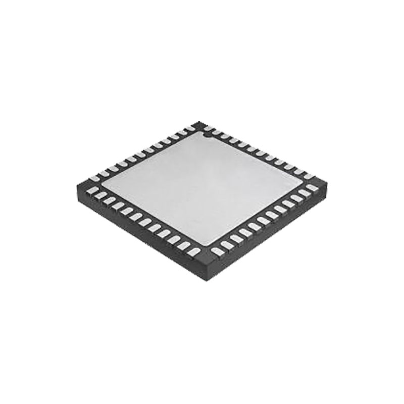
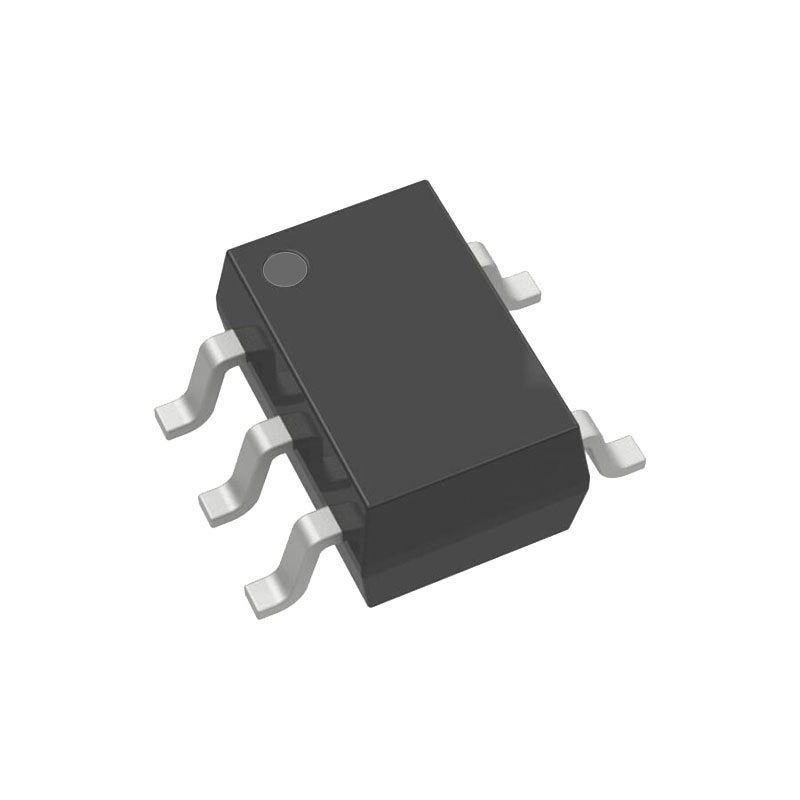
8-lead SOIC package with exposed paddle
Supported by ADIsimPower™ design tool
APPLICATIONS
Intermediate power rail conversion
DC-to-DC point of load applications
Communications and networking
Industrial and instrumentation
Healthcare and medical
Consumer
GENERAL DESCRIPTION
The ADP2302/ADP2303 are fixed frequency, current-mode control, step-down, dc-to-dc regulators with an integrated power MOSFET. The ADP2302/ADP2303 can run from an input voltage of 3.0 V to 20 V, which makes them suitable for a wide range of applications. The output voltage of the ADP2302/ ADP2303 can be down to 0.8 V for the adjustable version, while the fixed output version is available in preset output voltage options of 5.0 V, 3.3 V, and 2.5 V. The 700 kHz operating frequency allows small inductor and ceramic capacitors to be used, providing a compact solution. Current mode control provides fast and stable line and load transient performance.
The ADP2302/ADP2303 have integrated soft start circuitry to prevent a large inrush current at power-up. The power-good signal can be used to sequence devices that have an enable input. The precision enable threshold voltage allows the part to be easily sequenced from other input/output supplies. Other key features include undervoltage lockout (UVLO), overvoltage protection (OVP), thermal shutdown (TSD), and overcurrent protection (OCP).
The ADP2302/ADP2303 devices are available in the 8-lead, SOIC package with exposed paddle and are rated for the −40oC to +125oC junction temperature range.
THEORY OF OPERATION
The ADP2302/ADP2303 are nonsynchronous, step-down, dc-to-dc regulators, each with an integrated high-side power MOSFET. The high switching frequency and 8-lead SOIC package provide a small, step-down, dc-to-dc regulator solution.
The ADP2302/ADP2303 can operate with an input voltage from 3.0 V to 20 V while regulating an output voltage down to 0.8 V. The ADP2302 can provide 2 A maximum continuous output current, and the ADP2303 can provide 3 A maximum continuous output current.
BASIC OPERATION
The ADP2302/ADP2303 use the fixed-frequency, peak current mode PWM control architecture from medium to high loads, but shift to a pulse-skip mode control scheme at light loads to reduce the switching power losses and improve efficiency. When these devices operate in fixed-frequency PWM mode, output regulation is achieved by controlling the duty cycle of the integrated MOSFET. While the devices are operating in pulse-skip mode at light loads, the output voltage is controlled in a hysteretic manner with higher output ripple. In this mode of operation, the regulator periodically stops switching for a few cycles, thus keeping the conversion losses minimal to improve efficiency.
PWM MODE
In PWM mode, the ADP2302/ADP2303 operate at a fixed frequency, set by an internal oscillator. At the start of each oscillator cycle, the MOSFET switch is turned on, providing a positive voltage across the inductor. The inductor current increases until the current-sense signal crosses the peak inductor current threshold that turns off the MOSFET switch; this threshold is set by the error amplifier output. During the MOSFET off time, the inductor current declines through the external diode until the next oscillator clock pulse comes and a new cycle starts.
POWER SAVING MODE
To achieve higher efficiency, the ADP2302/ADP2303 smoothly transition to the pulse-skip mode when the output load decreases below the pulse-skip current threshold. When the output vol tage dips below the regulation, the ADP2302/ADP2303 enter PWM mode for a few oscillator cycles until the voltage increases to regulation range. During the idle time between bursts, the MOSFET switch is turned off, and the output capacitor supplies all the output current.
Because the pulse-skip mode comparator monitors the internal compensation node, which represents the peak inductor current information, the average pulse-skip load current threshold depends on the input voltage (VIN), the output voltage (VOUT), the inductor, and the output capacitor. 
Because the output voltage occasionally dips below regulation and then recovers, the output voltage ripple in the power saving mode is larger than the ripple in the PWM mode of operation.