FEATURES
Nonreflective 50 Ω design
Positive control range: 0 V to 3.3 V
Low insertion loss: 0.8 dB at 8.0 GHz
High isolation: 34 dB at 8.0 GHz
High power handling
33 dBm through path
27 dBm termination path
High linearity
1 dB compression (P1dB): 37 dBm typical
Input third-order intercept (IIP3): 58 dBm typical at 8.0 GHz
ESD rating: 4 kV human body model (HBM)
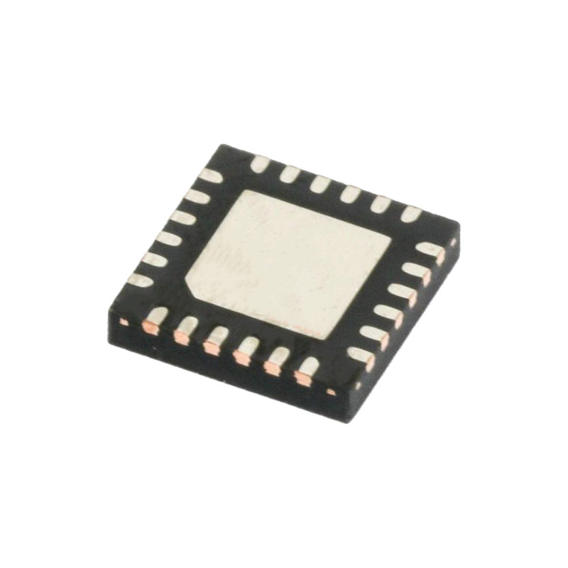
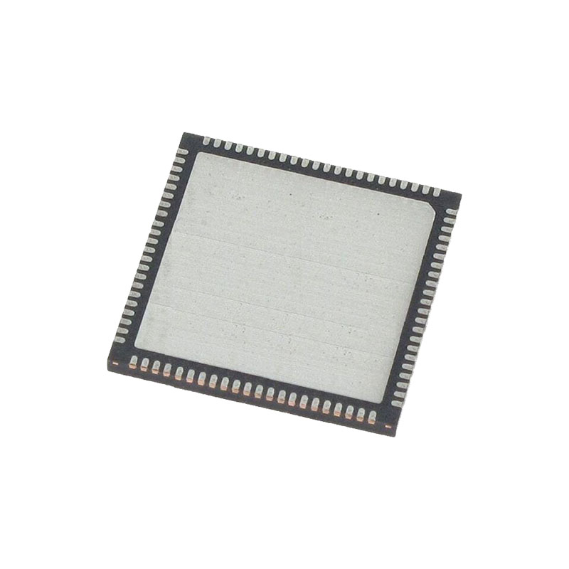
4 mm × 4 mm, 24-lead LFCSP package
No low frequency spurious
RF settling time (0.05 dB margin of final RFOUT): 9 µs
APPLICATIONS
Test instrumentation
Microwave radios and very small aperture terminals (VSATs)
Military radios, radars, and electronic counter measures (ECMs)
Fiber optics and broadband telecommunications
GENERAL DESCRIPTION
The ADRF5040 is a general-purpose, broadband high isolation, nonreflective single-pole, quad-throw (SP4T) switch in an LFCSP surface-mount package. Covering the 9 kHz to 12.0 GHz range, the switch offers high isolation and low insertion loss. The switch features 34 dB isolation and 0.8 dB insertion loss up to 8.0 GHz, and a 9 µs settling time of 0.05 dB margin of the final radio frequency output (RFOUT). The switch operates using positive control voltage of 3.3 V and 0 V and requires +3.3 V and −3.3 V supplies. The ADRF5040 is packaged in a 4 mm × 4 mm, surface-mount LFCSP package.
THEORY OF OPERATION
The ADRF5040 requires a positive supply voltage applied to the VDD pin and a negative voltage supply applied to the VSS pin. Bypassing capacitors are recommended on the supply lines to minimize RF coupling.
The ADRF5040 is controlled via two digital control voltages applied to the V1 pin and the V2 pin. A small value bypassing capacitor is recommended on these digital signal lines to improve the RF signal isolation.
The ADRF5040 is internally matched to 50 Ω at the RF input port (RFC) and the RF output ports (RF1, RF2, RF3, and RF4); therefore, no external matching components are required. TheRF1 through RF4 pins are dc-coupled, and dc blocking capacitors are required on the RF paths. The design is bidirectional; the input and outputs are interchangeable.
The ADRF5040 does not need any special power-up sequencing, and the relative order to power up the VDD and VSS supplies is not important. The V1 and V2 control signals can be applied only after VDD is powered up; this sequence avoids forward biasing and causing damage to the internal ESD protection circuits. Turn on the RF signal after the device supply settles to a steady state.
APPLICATIONS INFORMATION
EVALUATION BOARD
The ADRF5040-EVALZ evaluation board shown in Figure 27 is designed using proper RF circuit design techniques. Signal lines at the RF port have 50 Ω impedance, and the package ground leads and backside ground slug must be connected directly to the ground plane. The evaluation board is available from Analog Devices, Inc. upon request.

