GENERAL DESCRIPTION
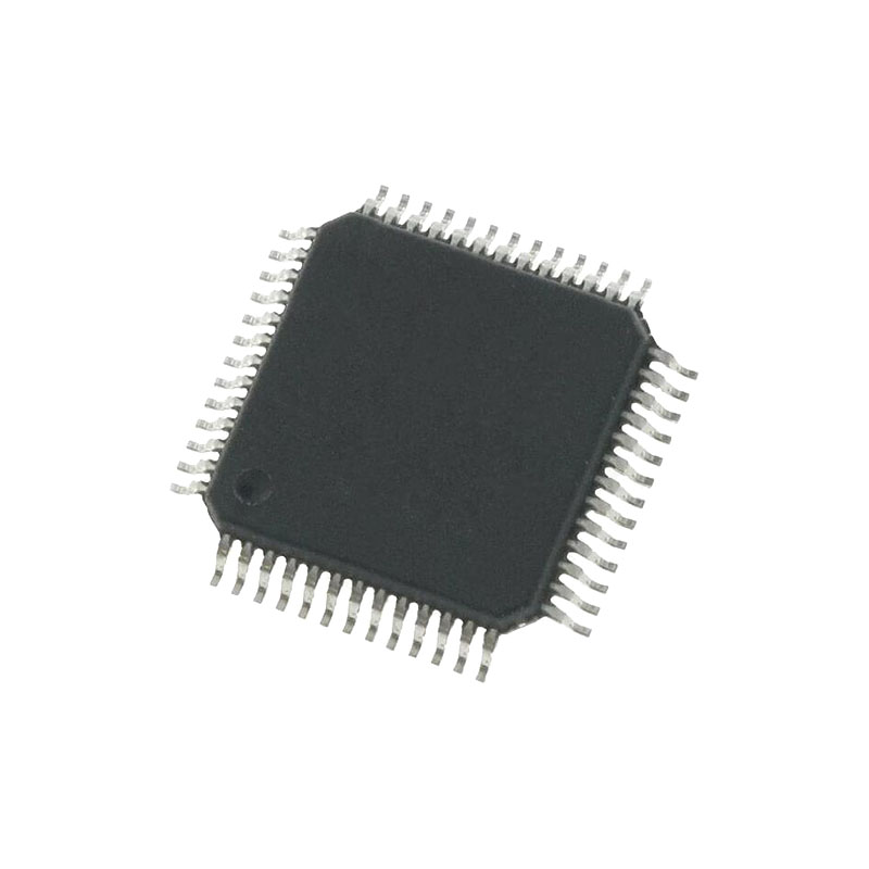
The ADuC841/ADuC842/ADuC8431 are complete smart transducer front ends, that integrates a high performance selfcalibrating multichannel ADC, a dual DAC, and an optimized single-cycle 20 MHz 8-bit MCU (8051 instruction set compatible) on a single chip. The ADuC841 and ADuC842 are identical with the exception of the clock oscillator circuit; the ADuC841 is clocked directly from an external crystal up to 20 MHz whereas the ADuC842 uses a 32 kHz crystal with an on-chip PLL generating a programmable core clock up to 16.78 MHz. The ADuC843 is identical to the ADuC842 except that the ADuC843 has no analog DAC outputs. The microcontroller is an optimized 8052 core offering up to 20 MIPS peak performance. Three different memory options are available offering up to 62 kBytes of nonvolatile Flash/EE program memory. Four kBytes of nonvolatile Flash/EE data memory, 256 bytes RAM, and 2 kBytes of extended RAM are also integrated on-chip.
FEATURES
Pin compatible upgrade of ADuC812/ADuC831/ADuC832
Increased performance
Single-cycle 20 MIPS 8052 core
High speed 420 kSPS 12-bit ADC
Increased memory
Up to 62 kBytes on-chip Flash/EE program memory
4 kBytes on-chip Flash/EE data memory
In-circuit reprogrammable
Flash/EE, 100 year retention, 100 kCycle endurance
2304 bytes on-chip data RAM
Smaller package
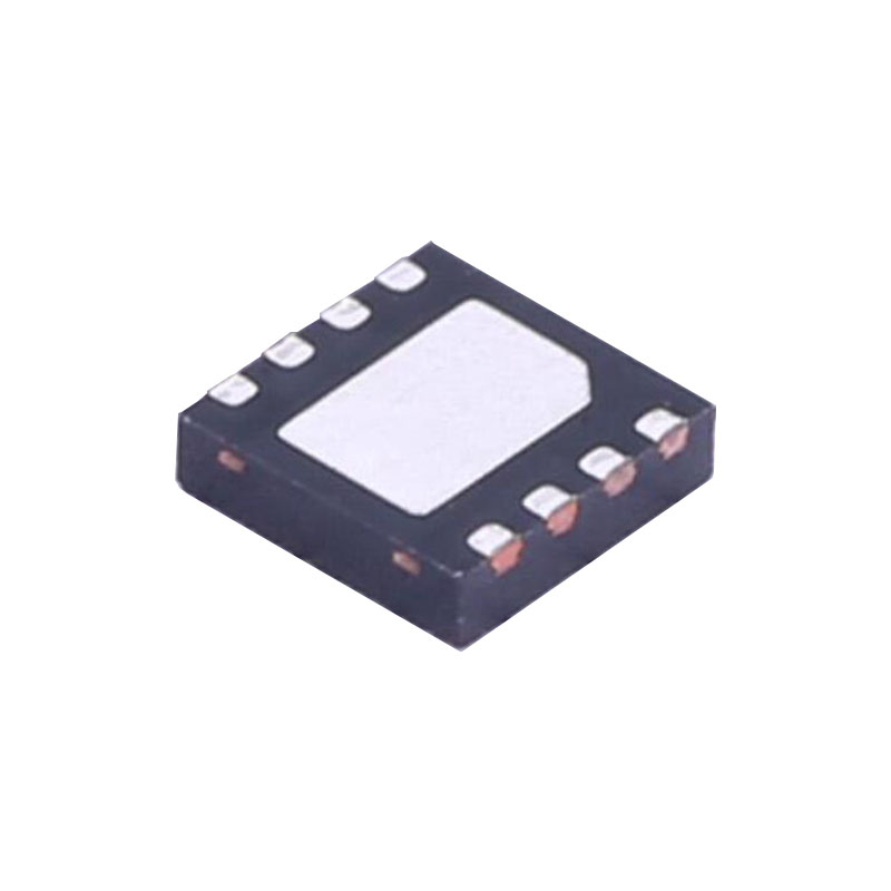
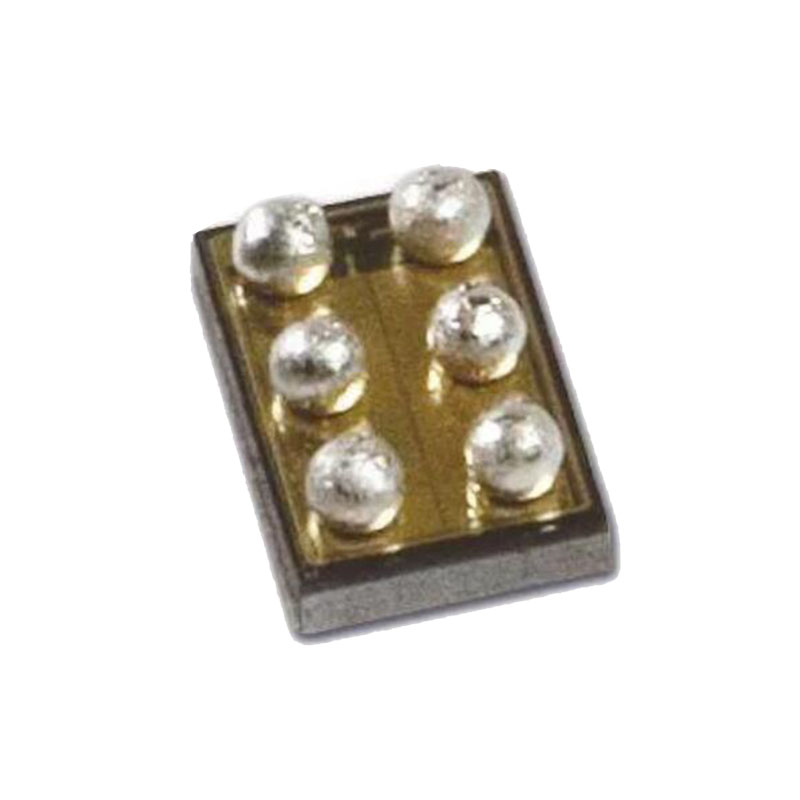
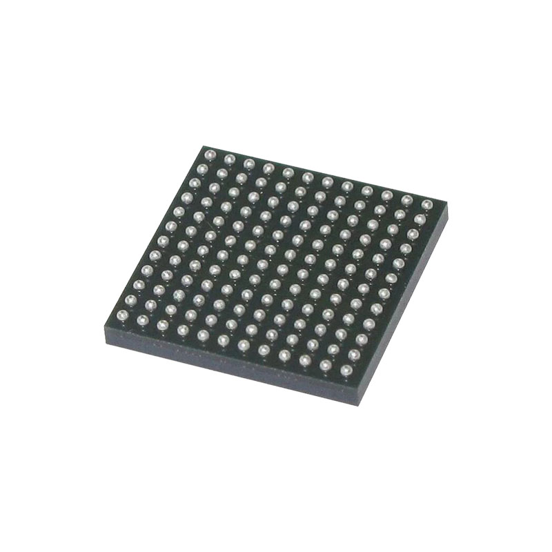
8 mm × 8 mm chip scale package
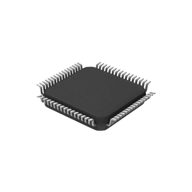
52-lead PQFP—pin-compatible upgrade Analog I/O
8-channel, 420 kSPS high accuracy, 12-bit ADC
On-chip, 15 ppm/°C voltage reference
DMA controller, high speed ADC-to-RAM capture
Two 12-bit voltage output DACs1
Dual output PWM ∑-∆ DACs
On-chip temperature monitor function
8052 based core
8051 compatible instruction set (20 MHz max)
High performance single-cycle core
32 kHz external crystal, on-chip programmable PLL
12 interrupt sources, 2 priority levels
Dual data pointers, extended 11-bit stack pointer
On-chip peripherals
Time interval counter (TIC)
UART, I2C, and SPI Serial I/O
Watchdog timer (WDT)
Power supply monitor (PSM)
Power
Normal: 4.5 mA @ 3 V (core CLK = 2.098 MHz)
Power-down: 10 µA @ 3 V2
Development tools
Low cost, comprehensive development system
incorporating nonintrusive single-pin emulation,
IDE based assembly and C source debugging
APPLICATIONS
Optical networking—laser power control
Base station systems
Precision instrumentation, smart sensors
Transient capture systems
DAS and communications systems
ADC CIRCUIT INFORMATION
General Overview
The ADC conversion block incorporates a fast, 8-channel, 12-bit, single-supply ADC. This block provides the user with multichannel mux, track-and-hold, on-chip reference, calibration features, and ADC. All components in this block are easily configured via a 3-register SFR interface. The ADC converter consists of a conventional successive approximation converter based around a capacitor DAC. The converter accepts an analog input range of 0 V to VREF. A high precision, 15 ppm, low drift, factory calibrated 2.5 V reference is provided on-chip. An external reference can be connected as described in the Voltage Reference Connections section. This external reference can be in the range 1 V to AVDD. Single-step or continuous conversion modes can be initiated in software or alternatively by applying a convert signal to an external pin. Timer 2 can also be configured to generate a repetitive trigger for ADC conversions. The ADC may be configured to operate in a DMA mode whereby the ADC block continuously converts and captures samples to an external RAM space without any interaction from the MCU core. This automatic capture facility can extend through a 16 MByte external data memory space. The ADuC841/ADuC842/ADuC843 are shipped with factory programmed calibration coefficients that are automatically downloaded to the ADC on power-up, ensuring optimum ADC performance. The ADC core contains internal offset and gain calibration registers that can be hardware calibrated to minimize system errors. A voltage output from an on-chip band gap reference proportional to absolute temperature can also be routed through the front end ADC multiplexer (effectively a 9th ADC channel input), facilitating a temperature sensor implementation.

