GENERAL DESCRIPTION
The ADuM4190 is ideal for linear feedback power supplies. The primary side controllers of the ADuM4190 enable improvements in transient response, power density, and stability as compared to commonly used optocoupler and shunt regulator solutions. Unlike optocoupler-based solutions, which have an uncertain current transfer ratio over lifetime and at high temperatures, the ADuM4190 transfer function does not change over its lifetime and is stable over a wide temperature range of −40°C to +125°C. Included in the ADuM4190 is a wideband operational amplifier for a variety of commonly used power supply loop compensation techniques. The ADuM4190 is fast enough to allow a feedback loop to react to fast transient conditions and overcurrent conditions. Also included is a high accuracy 1.225 V reference to compare with the supply output setpoint.
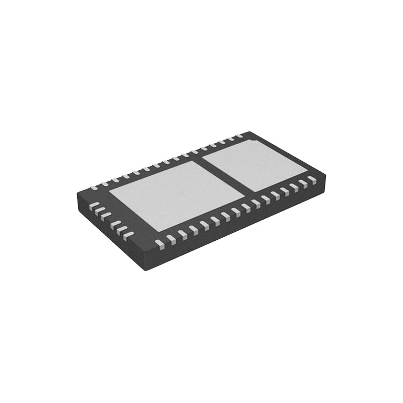
The ADuM4190 is packaged in a wide body, 16-lead SOIC package for a reinforced 5 kV rms isolation voltage rating.
FEATURES
Stable over time and temperature
0.5% initial accuracy
1% accuracy over the full temperature range
Compatible with Type II or Type III compensation networks
Reference voltage: 1.225 V
Compatible with DOSA
Low power operation: <7 mA total
Wide voltage supply range
VDD1: 3 V to 20 V
VDD2: 3 V to 20 V
Bandwidth: 400 kHz
Isolation voltage: 5 kV rms reinforced
Safety and regulatory approvals
UL 1577
VISO = 5000 V rms for 1 minute
IEC/EN 60950-1
IEC/CSA 60601-1
IEC/CSA 61010-1
CQC GB 4943.1
DIN EN IEC 60747-17 (VDE 0884-17)
VIORM = 645 V peak
Wide temperature range
−40°C to +125°C ambient operation
150°C maximum junction temperature
APPLICATIONS
Linear feedback power supplies
Inverters
Uninterruptible power supplies (UPS)
DOSA-compatible modules
Voltage monitors
APPLICATIONS INFORMATION
In the test circuits of the ADuM4190 , external supply voltages from 3 V to 20 V are provided to
the VDD1 and VDD2 pins, and internal regulators provide 3.0 V to operate the internal circuits of each side of the ADuM4190. An internal precision 1.225 V reference provides the reference for the ±1% accuracy of the isolated error amplifier. UVLO circuits monitor the VDDx supplies to turn on the internal circuits when the 2.8 V rising threshold is met and to turn off the error amplifier outputs to a high impedance state when VDDx falls below 2.6 V. The op amp on the right side of the ADuM4190 has a noninverting +IN pin and an inverting −IN pin available for connecting a feedback voltage in an isolated dc-to-dc converter output, usually through a voltage divider. The COMP pin is the op amp output, which can be used to attach resistor and capacitor components in a compensation network. The COMP pin internally drives the Tx transmitter block, which converts the op amp output voltage into an encoded output that is used to drive the digital isolator transformer. On the left side of the ADuM4190, the Rx block decodes the PWM signal that is output by the transformer and converts the signal into a voltage that drives an amplifier block; the amplifier block produces the error amplifier output available at the EAOUT pin. The EAOUT pin can deliver ±3 mA and has a voltage level from 0.4 V to 2.4 V, which is typically used to drive the input of a PWM controller in a dc-to-dc circuit. For an application that requires more output voltage to drive its controller, the EAOUT2 pin can be used . The EAOUT2 pin delivers up to ±1 mA with an output voltage of 0.6 V to 4.8 V for an output that has a pull-up resistor to a 5 V supply. If the EAOUT2 pull-up resistor is connected to a 10 V to 20 V supply, the output is specified to a minimum of 5.0 V to allow use with a PWM controller that requires a minimum input operation of 5 V.