GENERAL DESCRIPTION
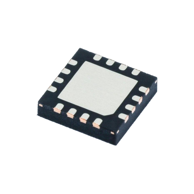
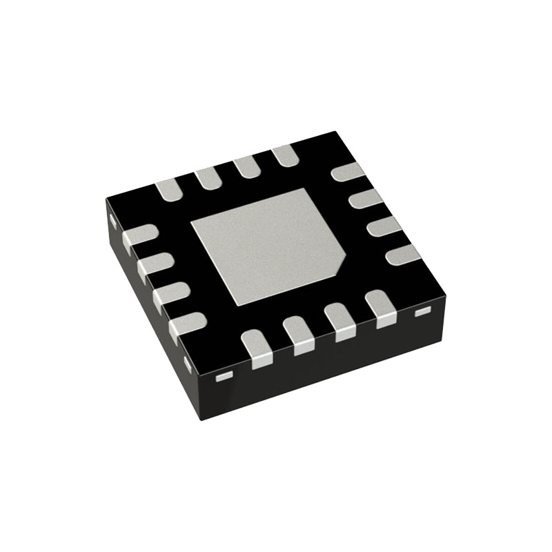
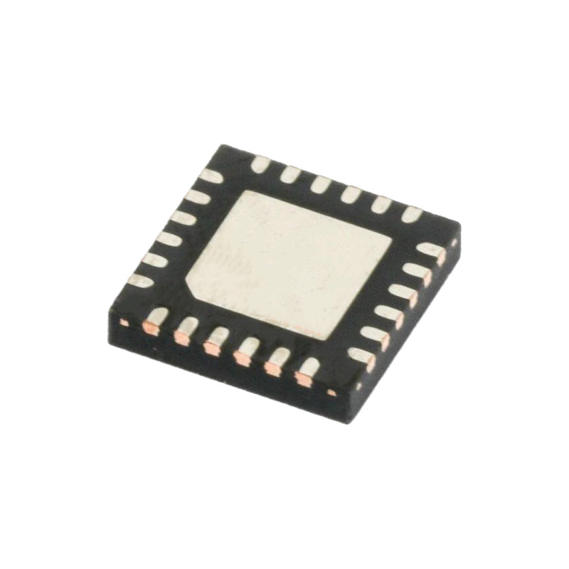
The HMC1118 is a general-purpose, broadband, nonreflective single-pole, double-throw (SPDT) switch in a LFCSP surface mount package. Covering the 9 kHz to 13.0 GHz range, the switch offers high isolation and low insertion loss. The switch features >48 dB isolation, 0.68 dB insertion loss up to 8.0 GHz, and a 7.5 μs settling time of 0.05 dB margin of final RFOUT. The switch operates using positive control voltage logic lines of +3.3 V and 0 V and requires +3.3 V and −2.5 V supplies. The HMC1118 can cover the same operating frequency range with a single positive supply voltage applied and the negative supply voltage (VSS) tied to ground and still maintaining good power handling performance. The HMC1118 is packaged in a 3 mm × 3 mm, surface mount LFCSP package.
FEATURES
Nonreflective 50Ωdesign
Positive control: 0 V/3.3 V
Low insertion loss: 0.68 dB at 8.0 GHz
High isolation: 48 dB at 8.0 GHz
High power handling
35 dBm through path
27 dBm terminated path
High linearity
1 dB compression (P1dB): 37 dBm typical
Input third-order intercept (IIP3): 62 dBm typical
ESD rating: 2 kV human body model (HBM)
3 mm × 3 mm, 16-lead LFCSP package
No low frequency spurious
Settling time (0.05 dB margin of final RFOUT): 7.5 μs
APPLICATIONS
Test instrumentation
Microwave radios and very small aperture terminals (VSATs)
Military radios, radars, and electronic counter measures (ECMs)
Fiber optics and broadband telecommunications
THEORY OF OPERATION
The HMC1118 requires a positive supply voltage applied to the VDD pin and a negative supply voltage applied to the VSS pin. Bypassing capacitors are recommended on the supply lines to minimize RF coupling.
The HMC1118 can operate with a single positive supply voltage applied to the VDD pin and the negative voltage input pin (VSS) connected to ground; however, some performance degradations in the input power compression and third-order intercept can occur.
The HMC1118 is controlled via two digital control voltages applied to the VCTRL pin and the LS pin. A small value bypassing capacitor is recommended on these digital signal lines to improve the RF signal isolation.
The HMC1118 is internally matched to 50Ωat the RF input port (RFC) and the RF output ports (RF1 and RF2); therefore, no external matching components are required. The RF1 and RF2 pins are dc-coupled, and dc blocking capacitors are required on the RF paths if the RF potential is not equal to a commonmode voltage of 0 V. The design is bidirectional; the input and outputs are interchangeable.
The ideal power-up sequence is as follows:
1. Power up GND.
2. Power up VDD and VSS. The relative order is not important.
3. Power up the digital control inputs. The relative order of the logic control inputs is not important. Powering the digital control inputs before the VDD supply can inadvertently forward bias and damage the internal ESD protection structures.
4. Power up the RF input.
The logic select (LS) allows the user to define the control input logic sequence for the RF path selections. With the LS pin set to logic high, the RFC to RF1 path turns on when VCTRL is logic low, and the RFC to RF2 path turns on when VCTRL is logic high. With LS set to logic low, the RFC to RF1 path turns on when VCTRL is logic high, and the RFC to RF2 path turns on when VCTRL is logic low.
Depending on the logic level applied to the LS and VCTRL pins, one RF output port (for example, RF1) is set to on mode, by which an insertion loss path provides the input to the output. The other RF output port (for example, RF2) is then set to off mode, by which the output is isolated from the input. When the RF output port (RF1 or RF2) is in isolation mode, internally terminate it to 50 Ω, and the port absorbs the applied RF signal.

