FEATURES
Attenuation range: 0.5 dB (LSB) steps to 31.5 dB ±0.5 dB typical step error
Low insertion loss: 2.8 dB at 4 GHz
High linearity at VEE = −3 V
Input P0.1dB: 22 dBm typical
Input IP3: 45 dBm typical
High RF input power handling: 25 dBm maximum
Low relative phase: 30° typical at 6.0 GHz
Single-supply operation: −3 V to −5 V
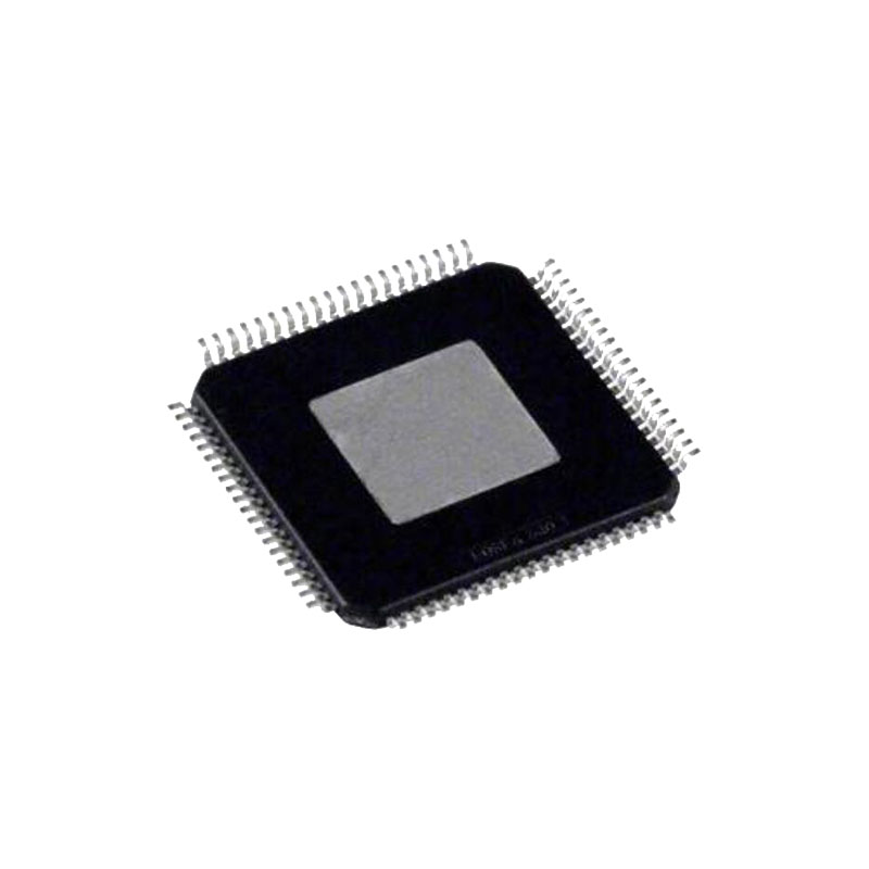
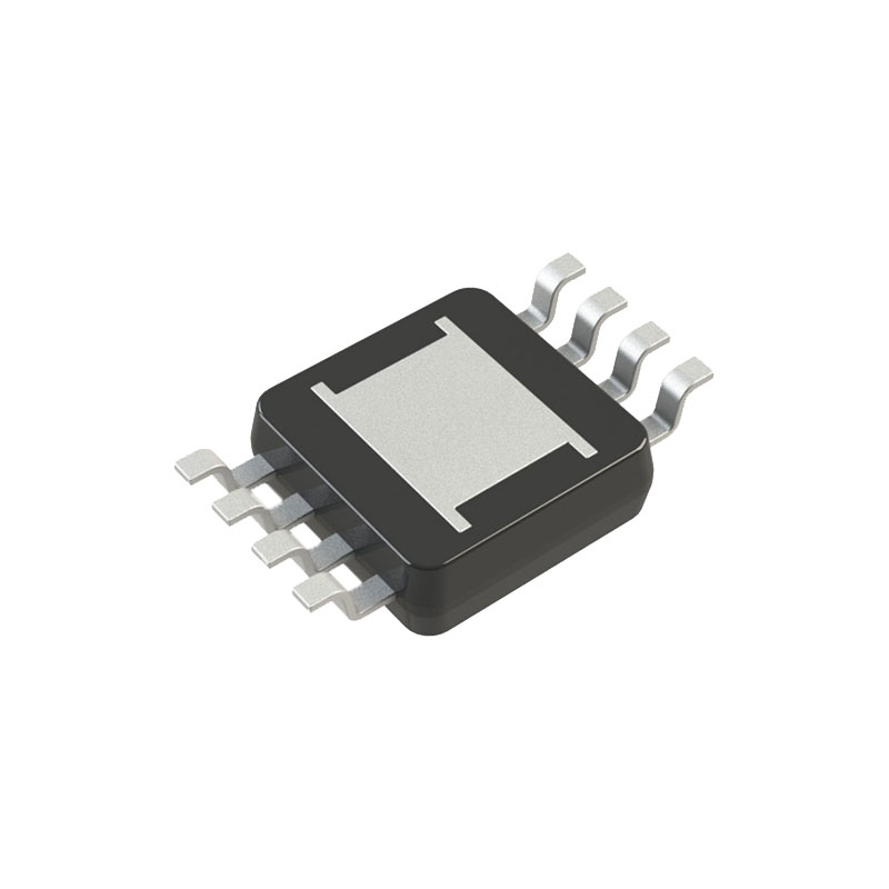
16-lead, 3 mm × 3 mm LFCSP package
APPLICATIONS
Cellular infrastructure
Microwave radios and very small aperture terminals (VSATs)
Test equipment and sensors
Intermediate frequency (IF) and RF designs
Military and space
GENERAL DESCRIPTION
The HMC424ALP3E is a broadband, 6-bit, gallium arsenide(GaAs), digital attenuator in low cost, leadless surface-mount package with a 31.5 dB attenuation control range in 0.5 dB steps.
The HMC424ALP3E offers excellent attenuation accuracy of ±(0.2 dB + 4% of attenuation state) and high input linearity with a typical insertion loss of less than 4 dB over the specified frequency range from 0.1 GHz to 13.0 GHz. The attenuator bit values are 0.5 dB (LSB), 1 dB, 2 dB, 4 dB, 8 dB, and 16 dB for a total attenuation of 31.5 dB with a ±0.5 dB typical step error.
The device allows a user to program the attenuation state via six parallel control inputs toggled between 0 V and VEE.
The HMC424ALP3E operates with a single negative supply voltage from −3 V to −5 V, and requires an external level shifter to interface with a CMOS/transistor to transistor logic (TTL) interface.
The HMC424ALP3E comes in a RoHS compliant, compact, 3 mm × 3 mm, 16-lead lead frame chip scale package (LFCSP).
THEORY OF OPERATION
The HMC424ALP3E incorporates a 6-bit attenuator die that offers an attenuation range of 31.5 dB in 0.5 dB steps. The attenuation state is changed by the parallel control voltage inputs (V1 to V6) directly.
The HMC424ALP3E allows the user to program the attenuation state via six parallel control inputs toggled between 0 V and VEE. When interfacing with a TTL/CMOS interface, an external level shifter is required. For example, a simple driver using standard logic ICs provides fast switching while using minimum dc current. The series resistance is recommended to suppress unwanted RF signals at the input of the V1 to V6 control lines.
POWER SUPPLY
The HMC424ALP3E requires a single dc voltage applied to the
VEE pin. The ideal power-up sequence is as follows:
1.Connect the ground reference.
2.Apply a supply voltage to the VEE pin.
3.Power up the digital control inputs. The relative order ofthe digital control inputs is not important.
4.Apply an RF input signal to RFIN.
RF INPUT AND OUTPUT
The attenuator in the HMC424ALP3E is bidirectional. The RFIN and RFOUT pins are interchangeable as the RF input and output ports. The attenuator is internally matched to 50 Ω at both the input and the output. Therefore, no external matching components are required.
The RF input and output pins of the HMC424ALP3E are internally dc biased to 0 V. Therefore, they require external dc blocking capacitors if the RF line potential is not equal to 0 V. Select the value of these dc blocking capacitors based on the minimum operating frequency. Use larger value capacitors to extend the operation to lower frequencies.
APPLICATIONS INFORMATION
EVALUATION BOARD
The HMC424ALP3E uses a 4-layer evaluation board. The copper thickness is 0.5 oz (0.7 mil) on each layer. The top dielectric material is 10 mil Rogers RO4350 for optimal high frequency performance, whereas the middle and bottom dielectric materials are FR4 type materials to achieve an overall board thickness of 62 mil. RF traces are routed on the top copper layer, and the bottom layer is a grounded plane that provides a solid ground for the RF transmission lines. The RF transmission lines are designed using a coplanar waveguide (CPWG) model with a width of 16 mil and ground spacing of 13 mil to have a characteristic impedance of 50 Ω. For enhanced RF and thermal grounding, as many plated through vias as possible are arranged around transmission lines and under the exposed pad of the package.