FEATURES
Low noise figure: 1.8 dB typical
High gain: 19.5 dB
High P1dB output power: 16 dBm typical
Single supply: 3.5 V at 80 mA
Output IP3: 28 dBm
50 Ω matched input/output
Self biased with optional bias control for quiescent drain
control (IDQ) reduction.
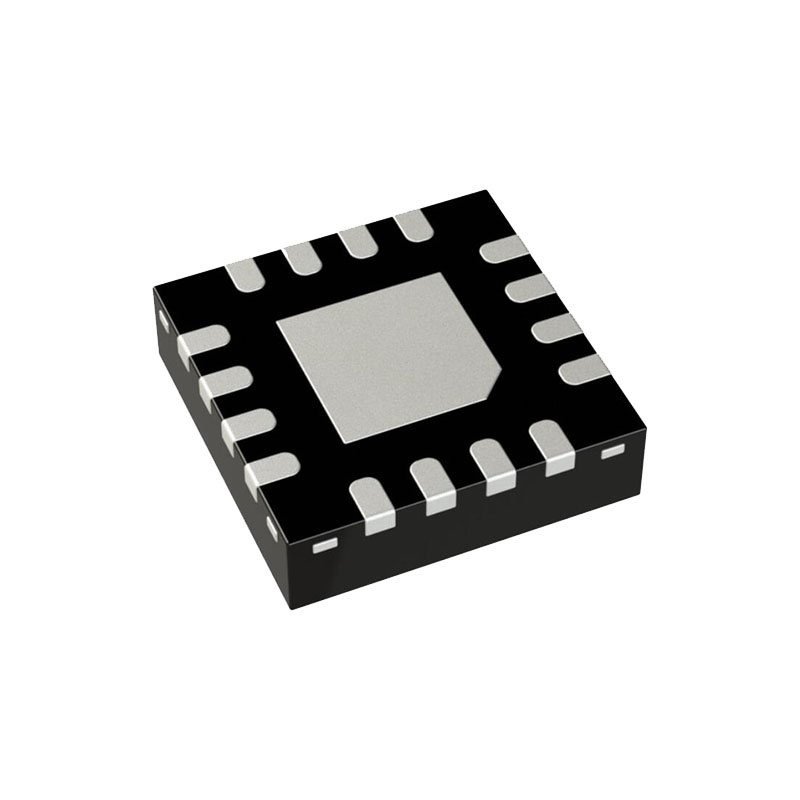
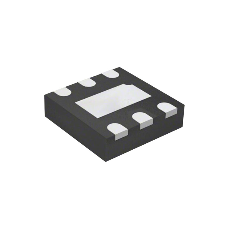
3 mm × 3 mm, 16-lead LFCSP: 9 mm²
APPLICATIONS
Point to point radios
Point to multi point radios
Military and space
Test instrumentation
GENERAL DESCRIPTION
The HMC902LP3E is a gallium arsenide (GaAs), pseudomorphic high electron mobility transistor (pHEMT), monolithic microwave integrated circuit (MMIC) low noise amplifier (LNA), which is self biased with optional bias control for IDQ reduction. The HMC902LP3E is housed in a leadless 3 mm × 3 mm plastic surface mount package. The amplifier operates between 5 GHz and 11 GHz, providing 19.5 dB of small signal gain, 1.8 dB noise figure, and 28 dBm of output IP3, while requiring only 80 mA from a 3.5 V supply.
The P1dB output power of 16 dBm enables the LNA to function as a local oscillator (LO) driver for balanced, I/Q, or image reject mixers. The HMC902LP3E also features inputs/outputs that are dc blocked and internally matched to 50 Ω, making it ideal for high capacity microwave radios and C band, very small aperture terminal (VSAT) applications.
THEORY OF OPERATION
The HMC902LP3E is a GaAs, MMIC, pHEMT, LNA. The HMC902LP3E amplifier uses two gain stages in series. The basic schematic for the amplifier is shown , which forms a LNA operating from 5 GHz to 11 GHz with excellent noise figure performance.
The HMC902LP3E has single-ended input and output ports with impe dances that are nominally equal to 50 Ω over the 5 GHz to 11 GHz frequency range. Consequently, the device can be directly inserted into a 50 Ω system with no required impedance matching circuitry, which also means multiple HMC902LP3E amplifiers can be cascaded back to back without the need for external matching circuitry.
The input and output impedances are sufficiently stable vs. variations in temperature and supply voltage that no impedance matching compensation is required.
It is critical to supply very low inductance ground connections to the package ground pad to ensure stable operation. To achieve optimal performance from the HMC902LP3E and to prevent damage to the device, do not exceed the absolute maximum ratings.
PPLICATIONS INFORMATION
The HMC902LP3E has VGG1 and VGG2 optional gate bias pins. When these pads are left open, the amplifier runs in self biased operation with typical IDQ = 80 mA. ,shows the basic connections for operating the HMC902LP3E in self biased operation mode. Both RFIN and RFOUT ports of HMC902LP3E have on-chip dc block capacitors, eliminating the need for external ac coupling capacitors.
When using the optional VGG1 and VGG2 gate bias pins, use the recommended bias sequencing to prevent damage to the amplifier.
The recommended bias sequence during power-up is as follows:
- Connect to GND.
- Set VGG1 and VGG2 to −2.0 V.
- Set VDD1 and VDD2 to 3.5 V.
- Increase VGG1 and VGG2 to achieve typical IDQ = 80 mA.
- Apply the RF signal.
The recommended bias sequence during power-down is as follows:
- Turn off the RF signal.
- Decrease VGG1 and VGG2 to −2.0 V to achieve typical IDQ = 0 mA.
- Decrease VDD1 and VDD2 to 0 V.
- Increase VGG1 and VGG2 to 0 V.
The bias conditions previously listed (VDD = 3.5 V and IDQ =80 mA) are the recommended operating points to achieve optimum performance. The data used in this data sheet was taken with the recommended bias conditions.
When using the HMC902LP3E with different bias conditions, different performance than what is shown in the Typical Performance Characteristics section can result. Decreasing the VDD level has negligible effect on gain and NF performance, but reduces the P1dB, For applications where the P1dB requirement is not stringent, the HMC902LP3E can be down biased to reduce power consumption.

