FEATURES
Wide Input Voltage Range: 3V to 80V
Low Quiescent Current: 7µA
Low Dropout Voltage: 350mV
Output Current: 20mA
LT3014HV Survives 100V Transients (2ms)
No Protection Diodes Needed
Adjustable Output from 1.22V to 60V
1µA Quiescent Current in Shutdown
Stable with 0.47µF Output Capacitor
Stable with Aluminum, Tantalum or Ceramic Capacitors
Reverse-Battery Protection
No Reverse Current Flow from Output
Thermal Limiting
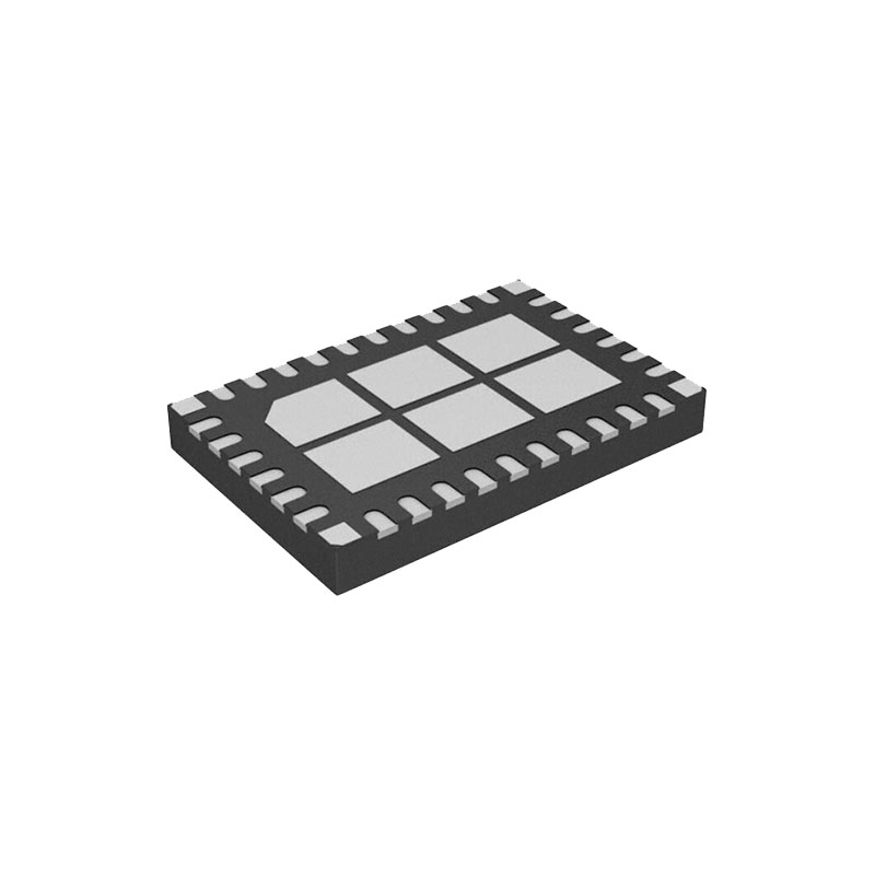
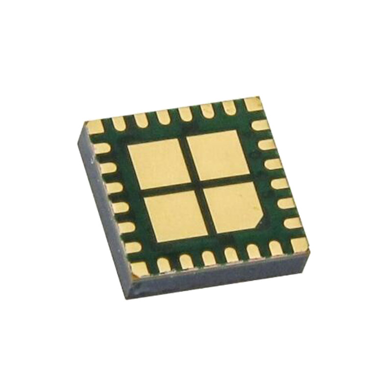
Available in 5-Lead ThinSOTTM and 8-Lead DFN Packages
APPLICATIONS
Low Current High Voltage Regulators
Regulator for Battery-Powered Systems
Telecom Applications
Automotive Applications
DESCRIPTION
The LT®3014 is a high voltage, micropower low dropout linear regulator. The device is capable of supplying 20mA of output current with a dropout voltage of 350mV. Designed for use in battery-powered or high voltage systems, the low quiescent current (7μA operating and 1μA in shutdown) makes the LT3014 an ideal choice. Quiescent current is also well controlled in dropout.
Other features of the LT3014 include the ability to operate with very small output capacitors. The regulators are stable with only 0.47μF on the output while most older devices require between 10μF and 100μF for stability. Small ceramic capacitors can be used without the necessary addition of ESR as is common with other regulators. Internal protec tion circuitry includes reverse-battery protection, current limiting, thermal limiting and reverse current protection.
The device is available as an adjustable device with a 1.22V reference voltage. The LT3014 regulator is available in the 5-lead ThinSOT and 8-lead DFN packages.
PIN FUNCTIONS
IN (Pin 1/Pin 8): Input. Power is supplied to the device through the IN pin. A bypass capacitor is required on this pin if the device is more than six inches away from the main input fi lter capacitor. In general, the output impedance of a battery rises with frequency, so it is advisable to include a bypass capacitor in battery-powered circuits. A bypass capacitor in the range of 0.1μF to 10μF is suffi cient. The LT3014 is designed to withstand reverse voltages on the IN pin with respect to ground and the OUT pin. In the case of a reversed input, which can happen if a battery is plugged in backwards, the LT3014 will act as if there is a diode in series with its input. There will be no reverse current fl ow into the LT3014 and no reverse voltage will appear at the load. The device will protect both itself and the load.
GND (Pin 2/Pins 4, 9): Ground.
SHDN (Pin 3/Pin 5):Shutdown. The SHDN pin is used to put the LT3014 into a low power shutdown state. The output will be off when the SHDN pin is pulled low. The SHDN pin can be driven either by 5V logic or open-collector logic with a pull-up resistor. The pull-up resistor is only required to supply the pull-up current of the open-collec tor gate, normally several microamperes. If unused, the SHDN pin must be tied to IN or to a logic high.
ADJ (Pin 4/Pin 2):Adjust. This is the input to the error amplifi er. This pin is internally clamped to ±7V. It has a bias current of 4nA which fl ows into the pin (see curve of ADJ Pin Bias Current vs Temperature in the Typical Performance Characteristics). The ADJ pin voltage is 1.22V referenced to ground, and the output voltage range is 1.22V to 60V.
OUT (Pin 5/Pin 1):Output. The output supplies power to the load. A minimum output capacitor of 0.47μF is required to prevent oscillations. Larger output capacitors will be required for applications with large transient loads to limit peak voltage transients. See the Applications Information section for more information on output capacitance and reverse output characteristics.