DESCRIPTION
The LT3015 series are low noise, low dropout, negative linear regulators with fast transient response. The devices supply up to 1.5A of output current at a typical dropout voltage of 310mV. Operating quiescent current is typically 1.1mA and drops to < 1µA in shutdown. Quiescent current is also well controlled in dropout. In addition to fast transient response, the LT3015 series exhibit very low output noise, making them ideal for noise sensitive applications.The LT3015 regulators are stable with a minimum 10µF output capacitor. Moreover, the regulator can use small ceramic capacitors without the necessary addition of ESR as is common with other regulators. Internal protection circuitry includes reverse output protection, precision current limit with foldback and thermal limit with hysteresis.
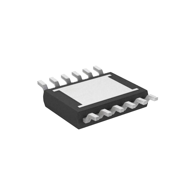
The LT3015 regulators are available in fixed output voltages of –2.5V, –3V, –3.3V, –5V,–12V and –15V and as an adjustable device with a –1.22V reference voltage. Packages include the 5-lead TO-220 and DD-Pak, a thermally enhanced 12-lead MSOP and the low profile (0.75 mm) 8-lead 3mm × 3mm DFN.
PIN FUNCTIONS
IN (Pins 1, 2, Exposed Pad Pin 9 / 1, 2, 3, 4, Exposed Pad Pin 13 / 3, Tab / 3, Tab ): Input. These pins supply power to the regulator. The Tab of the DD-Pak, TO-220 and the exposed backside pad of the DFN and MSOP packages is an electrical connection to IN and to the device’s substrate. For proper electrical and thermal performance, tie all IN pins together and tie IN to the exposed backside or Tab of the relevant package on the PCB. See the Applications Information Section for thermal considerations and calculating junction temperature. The LT3015 requires a bypass capacitor at IN. In general, a battery’s output impedance rises with frequency, so include a bypass capacitor in battery powered applications. An input bypass capacitor in the range of 1µF to 10µF generally suffices, but applications with large load transients may require higher input capacitance to prevent input supply droop and prevent the regulator from entering dropout.
SHDN (Pin 3 / 5 / 1 / 1): Shutdown. Use the SHDN pin to put the LT3015 into a micropower shutdown state. The SHDN function is bi-directional, allowing use of either positive or negative logic. The SHDN pin threshold voltages are referenced to GND. The output of the LT3015 is OFF if the SHDN pin is pulled typically within ±0.73V of GND. Driving the SHDN pin typically more than ±1.21V turns the LT3015 ON. Drive the SHDN pin with either a logic gate or with open collector/drain logic using a pull-up resistor. The resistor supplies the pull-up current of the open collector/drain gate, typically several microamperes.
The typical SHDN pin current is 2.8µA out of the pin (for negative logic) or 17µA into the pin (for positive logic). If the SHDN function is unused, connect the SHDN pin to VIN to turn the device ON. If the SHDN pin is floated, then the LT3015 is OFF. A parasitic diode exists between SHDNand IN of the LT3015. Therefore, do not drive the SHDN pin more than 0.3V below IN during normal operation or during a fault condition. The SHDN pin can also be used to set a programmable undervoltage lockout (UVLO) threshold for the regulator input supply.
GND (Pins 4, 5 / 6, 7 / 2 / 2): Ground. Tie all GND pin(s) together and tie the bottom of the output voltage setting resistor divider directly to the GND pin(s) for optimum load regulation performance.
ADJ (Pin 6 / 8 / 4 / 4): Adjust. For the adjustable voltage version, this pin is the error amplifier’s non-inverting input. It has a typical bias current of 30nA that flows into the pin. The ADJ pin reference voltage is –1.22V referred to GND, and the output voltage range is –1.22V to –29.5V. A parasitic substrate diode exists between ADJ and IN of the LT3015. Therefore, do not drive ADJ more than 0.3V below IN during normal operation or during a fault condition.