Description
The LTC2268-14 is 2-channel, simultaneous sampling 14-bit A/D converters designed for digitizing high frequency, wide dynamic range signals. They are perfect for demanding communications applications with AC performance that includes 73.1dB SNR and 88dB spurious free dynamic range (SFDR). Ultralow jitter of 0.15psRMS allows undersampling of IF frequencies with excellent noise performance.DC specs include ±1LSB INL (typ), ±0.3LSB DNL (typ) and no missing codes over temperature. The transition noise is a low 1.2LSBRMS.The digital outputs are serial LVDS to minimize the number of data lines. Each channel outputs two bits at a time (2-lane mode). At lower sampling rates there is a one bit per channel option (1-lane mode). The LVDS drivers have optional internal termination and adjustable output levels to ensure clean signal integrity.The ENC+ and ENC– inputs may be driven differentially or single-ended with a sine wave, PECL, LVDS, TTL, or CMOS inputs. An internal clock duty cycle stabilizer allows high performance at full speed for a wide range of clock duty cycles.
Features
2-Channel Simultaneous Sampling ADC
73.1dB SNR
88dB SFDR
Low Power: 299mW/243mW/203mW Total
150mW/121mW/101mW Per Channel
Single 1.8V Supply
Serial LVDS Outputs: 1 or 2 Bits Per Channel
Selectable Input Ranges: 1VP-P to 2VP-P 800MHz Full Power Bandwidth S/H
Shutdown and Nap Modes
Serial SPI Port for Configuration
Pin Compatible 14-Bit and 12-Bit Versions
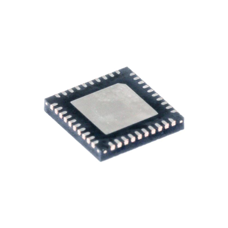
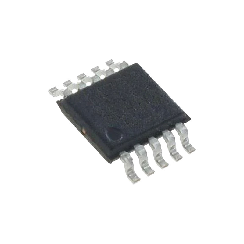
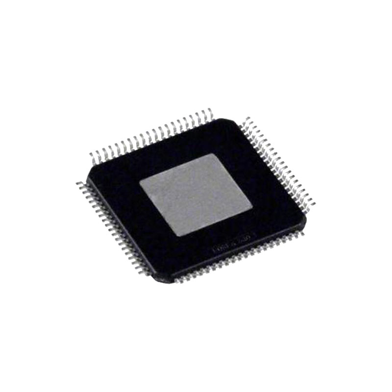
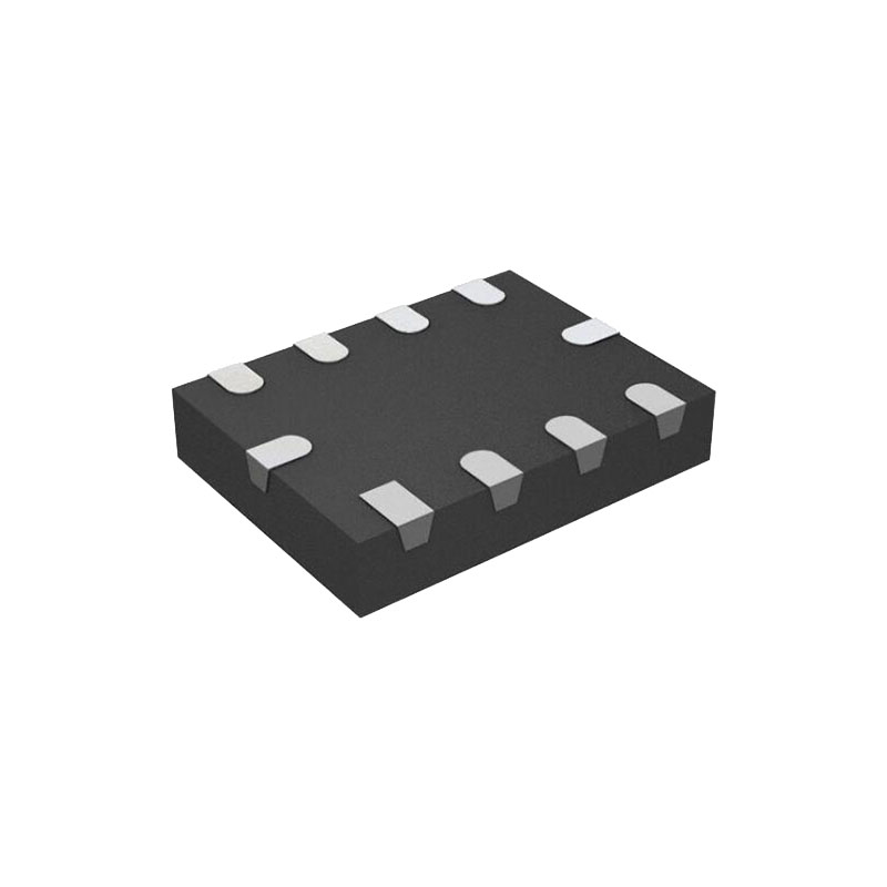
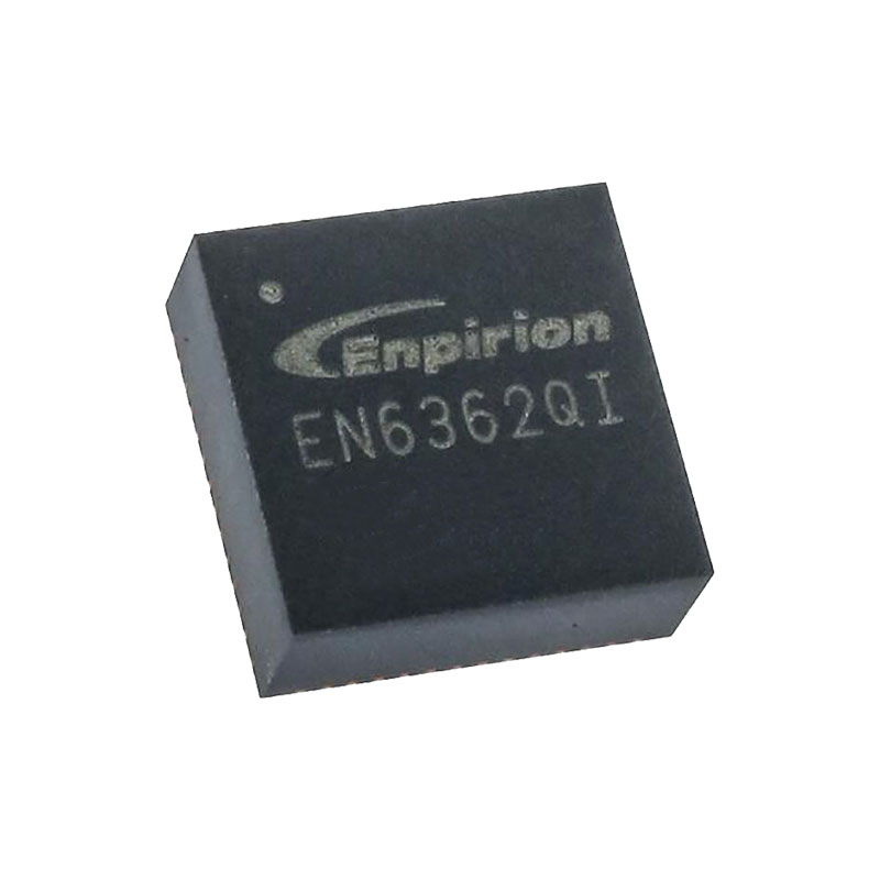
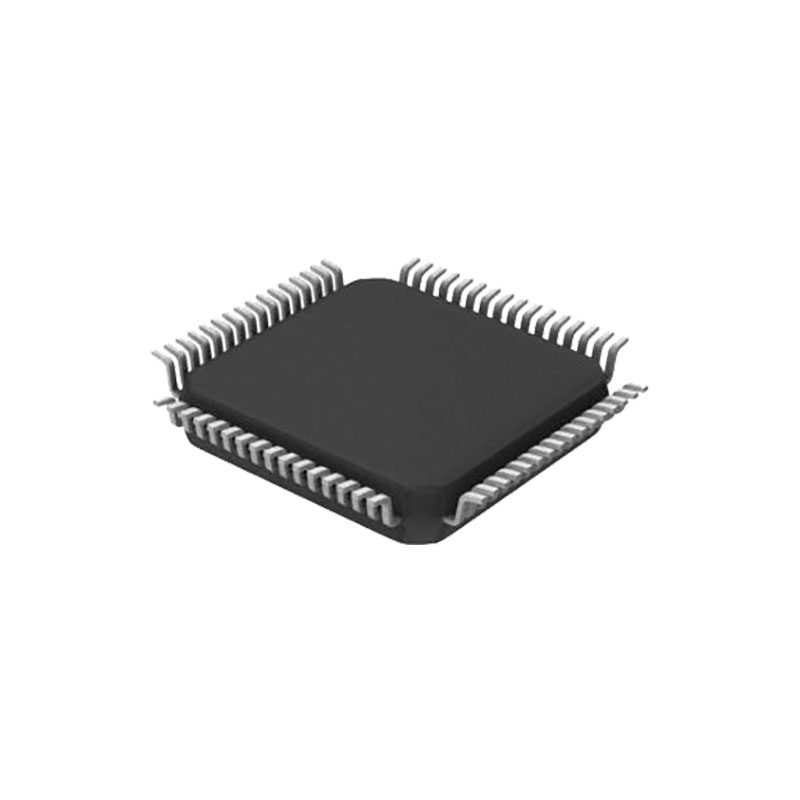
40-Pin (6mm × 6mm) QFN Package
Applications
Communications
Cellular Base Stations
Software Defined Radios
Portable Medical Imaging
Multichannel Data Acquisition
Nondestructive Testing
Applications information
CONVERTER OPERATION
The LTC2268-14 is low power, 2-channel, 14-bit, 125Msps/105Msps/80Msps A/D converters that are powered by a single 1.8V supply. The analog inputs should be driven differentially. The encode input can be driven differentially for optimal jitter performance, or single-ended for lower power consumption. To minimize the number of data lines the digital outputs are serial LVDS. Each channel outputs two bits at a time (2-lane mode). At lower sampling rates there is a one bit per channel option (1-lane mode). Many additional features can be chosen by programming the mode control registers through a serial SPI port.
ANALOG INPUT
The analog inputs are differential CMOS sample-and-hold circuits. The inputs should be driven differentially around a common mode voltage set by the VCM1 or VCM2 output pins, which are nominally VDD/2. For the 2V input range, the inputs should swing from VCM – 0.5V to VCM + 0.5V. There should be 180° phase difference between the inputs.
The two channels are simultaneously sampled by a shared encode circuit.
INPUT DRIVE CIRCUITS
Input filtering
If possible, there should be an RC lowpass filter right at the analog inputs. This lowpass filter isolates the drive circuitry from the A/D sample-and-hold switching, and also limits wideband noise from the drive circuitry. The RC component values should be chosen based on the application’s input frequency.
Digital Output Test Pattern
To allow in-circuit testing of the digital interface to the A/D, there is a test mode that forces the A/D data outputs (D13-D0) of both channels to known values. The digital output test patterns are enabled by serially programming mode control registers A3 and A4. When enabled, the test patterns override all other formatting modes: 2’s complement and randomizer.
Output Disable
The digital outputs may be disabled by serially programming mode control register A2. The current drive for all digital outputs including DCO and FR are disabled to save power or enable in-circuit testing. When disabled the common mode of each output pair becomes high impedance, but the differential impedance may remain low.
Sleep and Nap Modes
The A/D may be placed in sleep or nap modes to conserve power. In sleep mode the entire chip is powered down, resulting in 1mW power consumption. Sleep mode is enabled by mode control register A1 (serial programming mode), or by SDI (parallel programming mode). The amount of time required to recover from sleep mode depends on the size of the bypass capacitors on VREF, REFH, and REFL. In nap mode any combination of A/D channels can be powered down while theinternal reference circuits and the PLL stay active, allowing faster wake-up than from sleep mode. Recovering from nap mode requires at least 100 clock cycles. If the application demands very accurate DC settling then an additional 50µs should be allowed so the on-chip references can settle from the slight temperature shift caused by the change in supply current as the A/D leaves nap mode. Nap mode is enabled by mode control register A1 in the serial programming mode.

