DESCRIPTION
The LTC3412A is a high efficiency monolithic synchronous, step-down DC/DC converter utilizing a constant frequency, current mode architecture. It operates from an input voltage range of 2.25V to 5.5V and provides a regulated output voltage from 0.8V to 5V while delivering up to 3A of output current. The internal synchronous power switch with 77mΩ on-resistance increases efficiency and eliminates the need for an external Schottky diode. Switching frequency is set by an external resistor or can be synchronized to an external clock. 100% duty cycle provides low dropout operation extending battery life in portable systems. OPTI-LOOP® compensation allows the transient response to be optimized over a wide range of loads and output capacitors.
The LTC3412A can be configured for either Burst Mode operation or forced continuous operation. Forced continuous operation reduces noise and RF interference while Burst Mode operation provides high efficiency by reducing gate charge losses at light loads. In Burst Mode operation, external control of the burst clamp level allows the output voltage ripple to be adjusted according to the application requirements.
FEATURES
High Efficiency: Up to 95%
3A Output Current
Low Quiescent Current: 64µA
Low RDS(ON) Internal Switch: 77mΩ
2.25V to 5.5V Input Voltage Range
Programmable Frequency: 300kHz to 4MHz
±2% Output Voltage Accuracy
0.8V Reference Allows Low Output Voltage
Selectable Forced Continuous/Burst Mode® Operation with Adjustable Burst Clamp
Synchronizable Switching Frequency
Low Dropout Operation: 100% Duty Cycle
Power Good Output Voltage Monitor
Overtemperature Protected
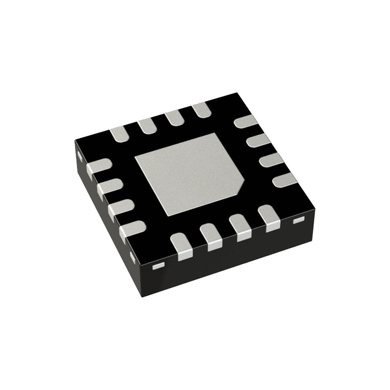
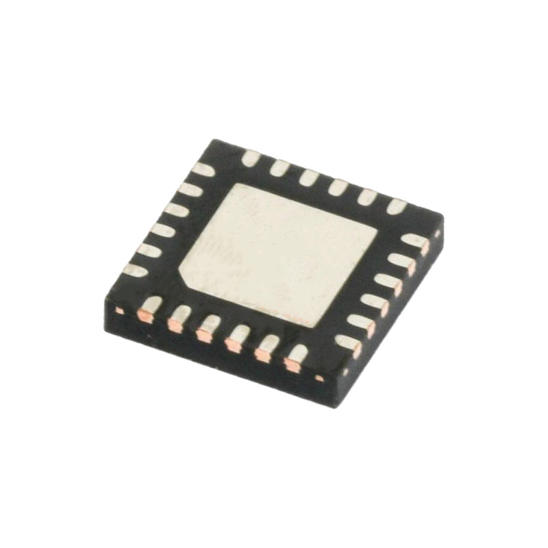
Available in 16-Lead Exposed Pad TSSOP and QFN Packages
APPLICATIONS
Point-of-Load Regulation
Notebook Computers
Portable Instruments
Distributed Power Systems
OPERATION
Main Control Loop
The LTC3412A is a monolithic, constant-frequency, current mode step-down DC/DC converter. During normal operation, the internal top power switch (P-channel MOSFET) is turned on at the beginning of each clock cycle. Current in the inductor increases until the current comparator trips
and turns off the top power MOSFET. The peak inductor current at which the current comparator shuts off the top power switch is controlled by the voltage on the ITH pin. The error amplifier adjusts the voltage on the ITH pin by comparing the feedback signal from a resistor divider on the VFB pin with an internal 0.8V reference. When the load current increases, it causes a reduction in the feedback voltage relative to the reference. The error amplifier raises the ITH voltage until the average inductor current matches the new load current. When the top power MOSFET shuts off, the synchronous power switch (N-channel MOSFET) turns on until either the bottom current limit is reached or the beginning of the next clock cycle. The bottom current limit is set at –1.3A for forced continuous mode and 0A for Burst Mode operation.
Frequency Synchronization
The internal oscillator of the LTC3412A can be synchronized to an external clock connected to the SYNC/MODE pin. The frequency of the external clock can be in the range of 300kHz to 4MHz. For this application, the oscillator timing resistor should be chosen to correspond to a frequency that is 25% lower than the synchronization frequency. During synchronization, the burst clamp is set to 0V, and each switching cycle begins at the falling edge of the clock signal.
Low Supply Operation
The LTC3412A is designed to operate down to an input supply voltage of 2.25V. One important consideration at low input supply voltages is that the RDS(ON) of the P-channel and N-channel power switches increases. The user should calculate the power dissipation when the LTC3412A is used at 100% duty cycle with low input voltages to ensure that thermal limits are not exceeded.
Slope Compensation and Inductor Peak Current
Slope compensation provides stability in constant frequency architectures by preventing subharmonic oscillations at duty cycles greater than 50%. It is accomplished internally by adding a compensating ramp to the inductor current signal at duty cycles in excess of 40%. Normally, the maximum inductor peak current is reduced when slope compensation is added. In the LTC3412A, however, slope compensation recovery is implemented to keep the maximum inductor peak current constant throughout the range of duty cycles. This keeps the maximum output current relatively constant regardless of duty cycle.

