DESCRIPTION
The LTM4651 is an ultralow noise, 58V, 24W DC/DC μModule inverting topology regulator. It regulates a negative output voltage (VOUT –) from a positive input supply voltage (VIN), and is designed to meet the radiated emissions requirements of EN55022. Conducted emission requirements can be met by adding standard filter components. Included in the package are the switching controller, power MOSFETs, inductor, filters and support components.
The LTM4651 can regulate VOUT – to a value between –0.5V and –26.5V, provided that its input and output voltages adhere to the safe operating area criteria of the LTM4651: VIN + |VOUT –| ≤ 58V. A switching frequency range of 250kHz to 3MHz is supported (400kHz default) and the module can synchronize to an external clock.
Despite being an inverting topology regulator, no level shift circuitry is needed to interface to the LTM4651’s RUN, PGOOD or CLKIN pins; those pins are referenced to GND.
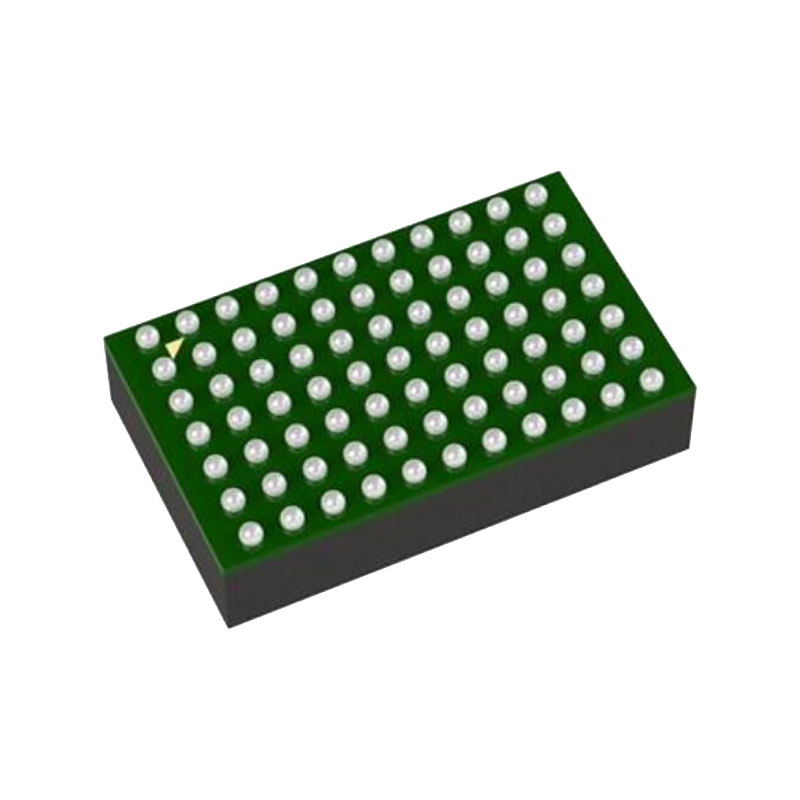
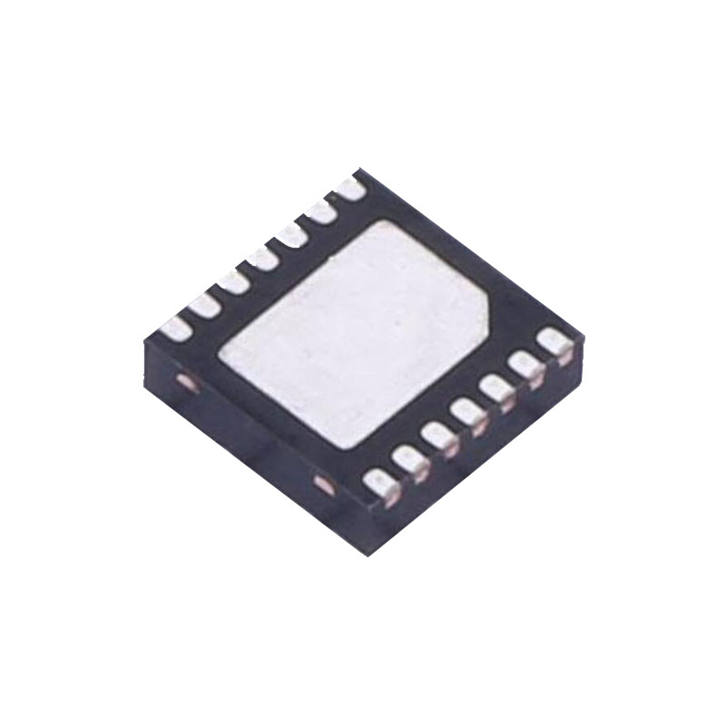
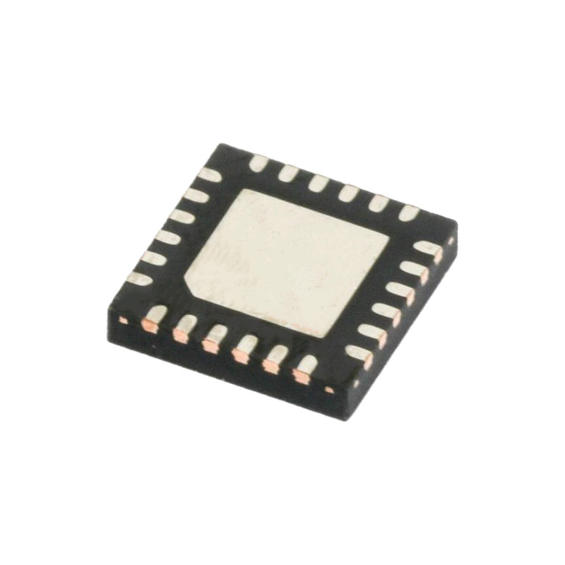
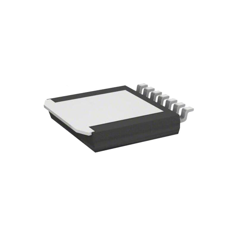
The LTM4651 is offered in a 15mm × 9mm × 5.01mm BGA package with SnPb or RoHS compliant terminal finish.
FEATURES
Complete Low EMI Switch Mode Power Supply
EN55022 Class B Compliant
Wide Input Voltage Range: 3.6V to 58V
Up to 4A Output Current
24W Output from 12VIN to –24VOUT, PLOSS = 5W, TA = 60°C, tRISE = 60°C, 200LFM
Output Voltage Range: –26.5V ≤ VOUT– ≤ –0.5V
Safe Operating Area: VIN + |VOUT–| ≤ 58V
±1.67% Total DC Output Voltage Error Over Line, Load and Temperature (–40°C to 125°C)
Parallel and Current Share with Multiple LTM4651s
Constant-Frequency Current Mode Control
Frequency Synchronization Range: 250kHz to 3MHz
Power Good Indicator and Programmable Soft-Start
Overcurrent/Overvoltage/Overtemperature Protection
15mm × 9mm × 5.01mm BGA Package
APPLICATIONS
Avionics, Industrial Control and Test Equipment
Video, Imaging and Instrumentation
48V Telecom and Network Power Supplies
RF Systems
OPERATION
Power Module Description
The LTM4651 is a non-isolated switch mode DC/DC power supply. It can provide up to 4A output current with a few external input and output capacitors. Set by a single resistor, RSET, the LTM4651 regulates a negative output voltage, VOUT –. VOUT – can be set to as low as –26.5V to as high as –0.5V. The LTM4651 operates from a positive input supply rail, VIN, between 3.6V and 58V. The LTM4651’s safe operating area is defined by: VIN + |VOUT –| ≤ 58V. The output current capability of the LTM4651 is dependent on VIN and VOUT. Though the LTM4651 is a ground-referred buck converter topology—also known as a two-switch buckboost converter—it contains built-in level-shift circuitry so that the RUN, CLKIN, and PGOOD pins are conveniently referred to GND (not VOUT –).
The LTM4651 contains an integrated constant-frequency current mode regulator, power MOSFETs, power inductor, EMI filter and other supporting discrete components. The nominal switching frequency range is from 400kHz to 3MHz, and the default operating frequency is 400kHz. It can be externally synchronized to a clock, from 250kHz to 3MHz.
The LTM4651 supports internal and external control loop compensation. Internal loop compensation is selected by connecting the COMPa and COMPb pins. Using internal loop compensation, the LTM4651 has sufficient stability margins and good transient performance with a wide range of output capacitors, even ceramic-only output capacitors. LTpowerCAD is available for transient load step and stability analysis.
Input filter and noise cancellation circuitry reduces noisecoupling to the module’s inputs and outputs, ensuring the module’s electromagnetic interference (EMI) meets the limits of EN55022 Class B.
Pulling the RUN pin below 1.2V forces the LTM4651 into a shutdown state. A capacitor can be applied from ISETa to SVOUT – to program the output voltage ramp-rate; or, the default LTM4651 ramp-rate can be set by connecting ISETa to ISETb; or, voltage tracking can be implemented by interfacing rail voltages to the ISETa pin.
Multiphase operation can be employed by applying an external clock source to the LTM4651’s synchronization input, the CLKIN pin.
LDO losses within the module are reduced by connecting EXTVCC to PGND through an RC-filter or by connecting EXTVCC to a suitable voltage source.
The LTM4651 also features a spare control pin called VINREG which can be used to reduce the input current draw during input line sag (“brownout”) conditions. Connect VINREG to INTVCC when this feature is not needed.

