DESCRIPTION
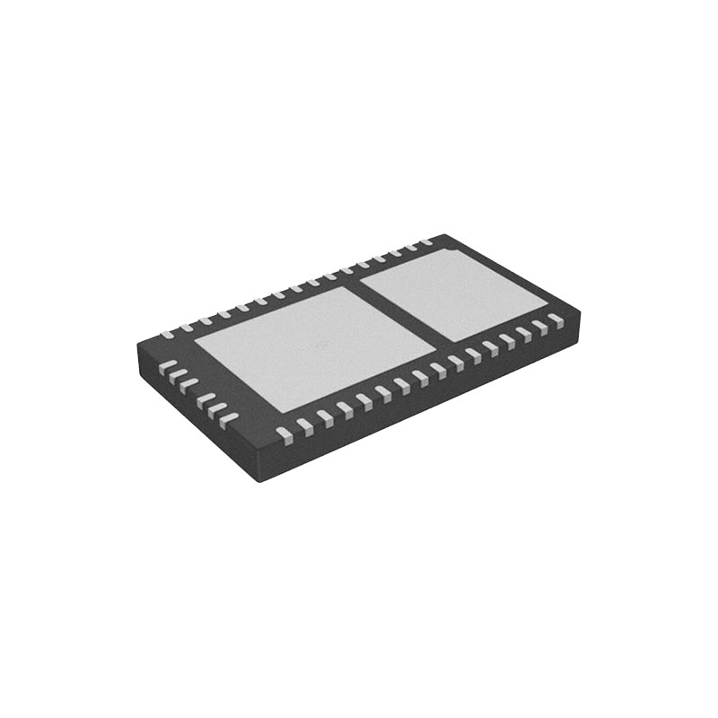
The LTM4675 is a dual 9A or single 18A step-down µModule® (micromodule) DC/DC regulator with 40ms turn-on time. It features remote configurability and telemetry-monitoring of power management parameters over PMBus— an open standard I2C-based digital interface protocol . The LTM4675 is comprised of fast analog control loops, precision mixed-signal circuitry, EEPROM, power MOSFETs, inductors and supporting components. The LTM4675’s 2-wire serial interface allows outputs to be margined, tuned and ramped up and down at programmable slew rates with sequencing delay times. Input and output currents and voltages, output power, temperatures, uptime and peak values are readable. Custom configuration of the EEPROM contents is not required. At start-up, output voltages, switching frequency, and channel phase angle assignments can be set by pin-strapping resistors. The LTpowerPlayGUI and DC1613 USB-to-PMBus converter and demo kits are available. The LTM4675 is offered in a 16mm × 11.9mm × 3.51mm BGA package available with SnPb or RoHS compliant terminal finish.
FEATURES
Dual, Fast, Analog Loops with Digital Interface for Control and Monitoring
Wide Input Voltage Range: 4.5V to 17V
Output Voltage Range: 0.5V to 5.5V
±0.5% Maximum DC Output Error Over Temperature
±2.5% Current Readback Accuracy at 9A Load
400kHz PMBus-Compliant I2C Serial Interface
Integrated 16-Bit ∆Σ ADC
Supports Telemetry Polling Rates Up to 125Hz
Constant Frequency Current Mode Control
Parallel and Current Share Multiple Modules
All 7-Bit Slave Addresses Supported
16mm × 11.9mm × 3.51mm BGA Package
Readable Data:
Input and Output Voltages, Currents, and Temperatures
Running Peak Values, Uptime, Faults and Warnings
Onboard EEPROM Fault Log Record with ECC
Writable Data and Configurable Parameters:
Output Voltage, Voltage Sequencing and Margining
Digital Soft-Start/Stop Ramp
OV/UV/OT, UVLO, Frequency and Phasing
System Optimization in Prototype and Production
APPLICATIONS INFORMATION
VIN TO VOUT STEP-DOWN RATIOS
There are restrictions in the maximum VIN and VOUT stepdown ratio that can be achieved for a given input voltage. Each output of the LTM4675 is capable of 95% duty cycle at 500kHz, but the VIN to VOUT minimum dropout is still a function of its load current and will limit output current capability related to high duty cycle on the topside switch. Minimum on-time tON(MIN) is another consideration in operating at a specified duty cycle while operating at a certain frequency due to the fact that tON(MIN) < D/fSW, where D is duty cycle and fSW is the switching frequency. tON(MIN) is specified in the electrical parameters as 45ns. See Note 6 in the ElectricalCharacteristics section for output current guideline.
INPUT CAPACITORS
The LTM4675 module should be connected to a low ACimpedance DC source. For the regulator input four 22µF input ceramic capacitors are used to handle the RMS ripple current. A 47µF to 100µF surface mount aluminum electrolytic bulk capacitor can be used for more input bulk capacitance. This bulk input capacitor is only needed if the input source impedance is compromised by long inductive leads, traces or not enough source capacitance. If low impedance power planes are used, then this bulk capacitor is not needed.
LIGHT LOAD CURRENT OPERATION
The LTM4675 has two modes of operation: high efficiency, discontinuous conduction mode or forced continuous conduction mode. The mode of operation is configured by bit 0 of the MFR_PWM_MODEn command (discontinuous conduction is always the start-up mode, forced continuous is the default running mode) If a channel is enabled for discontinuous mode operation, the inductor current is not allowed to reverse. The reverse current comparator, IREV , turns off the bottom MOSFET (MBn) just before the inductor current reaches zero, preventing it from reversing and going negative. Thus, the controller can operate in discontinuous(pulse-skippng) operation. In forced continuous operation, the inductor current is allowed to reverse at light loads or under large transient conditions. The peak inductor current is determined solely by the voltage on the COMPna pin. In this mode, the efficiency at light loads is lower than discontinuous mode operation. However, continuous mode exhibits lower output ripple and less interference with audio circuitry. Forced continuous conduction mode may result in reverse inductor current, which can cause the input supply to boost. The VIN_OV_FAULT_LIMIT can detect this (if SVIN is connected to VIN0 and/or VIN1) and turn off the offending channel. However, this fault is based on an ADC read and can nominally take up to 90ms to detect. If there is a concern about the input supply boosting, keep the part in discontinuous conduction operation.