General Description
The MCP1415/16 devices are high-speed, dual MOSFET drivers that are capable of providing up to 1.5A of peak current while operating from a single 4.5V to 18V supply. The inverting or noninverting single channel output is directly controlled from either TTL or CMOS (3V to 18V) logic. These devices also feature low shoot-through current, matched rise and fall time, and short propagation delays which make them ideal for high switching frequency applications. They provide low enough impedances in both the ‘On’ and ‘Off’ states to ensure the intended state of the MOSFET is not affected, even by large transients.
These devices are highly latch-up resistant under any condition within their power and voltage ratings. They are not subject to damage when noise spiking (up to 5V, of either polarity) occurs on the Ground pin. They can accept up to 500 mA of reverse current being forced back into their outputs without damage or logic upset. All terminals are fully protected against electrostatic discharge (ESD) up to 2.0 kV (HBM) and 300V (MM).
The MCP1415/16 is AEC-Q100 qualified for automotive applications.
Features
• Passes Automotive AEC-Q100 Reliability Testing
• High Peak Output Current: 1.5A (typical)
• Wide Input Supply Voltage Operating Range:
– 4.5V to 18V
• Low Shoot-Through/Cross-Conduction Current in Output Stage
• High Capacitive Load Drive Capability:
– 470 pF in 13 ns (typical)
– 1000 pF in 18 ns (typical)
• Short Delay Times: 44 ns (tD1), 47 ns (MCP1415 tD2), 54 ns (MCP1416 tD2) (typical)
• Low Supply Current:
– With Logic ‘1’ Input – 0.65 mA (typical)
– With Logic ‘0’ Input – 0.1 mA (typical)
• Latch-Up Protected: Withstands 500 mA Reverse Current
• Logic Input Withstands Negative Swing up to 5V
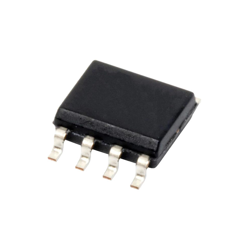
• Space-Saving 5-Lead SOT-23 Package
Applications
• Switch Mode Power Supplies
• Pulse Transformer Drive
• Line Drivers
• Level Translator
• Motor and Solenoid Drive
Supply Input (VDD)
VDD is the bias supply input for the MOSFET driver and has a voltage range of 4.5V to 18V. This input must be decoupled to ground with a local capacitor. This bypass capacitor provides a localized low-impedance path for the peak currents that are provided to the load.
Control Input (IN)
The MOSFET driver input is a high-impedance, TTL/CMOS compatible input. The input also has hysteresis between the high and low input levels, allowing them to be driven from slow rising and falling signals and to provide noise immunity.
Ground (GND)
Ground is the device return pin. The ground pin should have a low-impedance connection to the bias supply source return. When the capacitive load is being discharged, high peak currents will flow out of the ground pin.
General Information
MOSFET drivers are high-speed, high-current devices which are intended to source/sink high peak currents to charge/discharge the gate capacitance of external MOSFETs or Insulated-Gate Bipolar Transistors (IGBTs). In high frequency switching power supplies, the Pulse-Width Modulation (PWM) controller may not have the drive capability to directly drive the power MOSFET. A MOSFET driver such as the MCP1415/16 family can be used to provide additional source/sink current capability.
Decoupling Capacitors
Careful layout and decoupling capacitors are required when using power MOSFET drivers. Large current is required to charge and discharge capacitive loads quickly. For example, approximately 720 mA are needed to charge a 1000 pF load with 18V in 25 ns.
To operate the MOSFET driver over a wide frequency range with low supply impedance, it is recommended to place a ceramic and a low ESR film capacitor in parallel between the driver VDD and GND. A 1.0 µF low ESR film capacitor and a 0.1 µF ceramic capacitor placed between pins 2 and 4 are required for reliable operation. These capacitors should be placed close to the driver to minimize circuit board parasitics and provide a local source for the required current.