GENERAL DESCRIPTION
The REF19x series precision band gap voltage references use a patented temperature drift curvature correction circuit and laser trimming of highly stable, thin-film resistors to achieve a very low temperature coefficient and high initial accuracy.
The REF19x series is made up of micropower, low dropout voltage (LDV) devices, providing stable output voltage from supplies as low as 100 mV above the output voltage and consuming less than 45 μA of supply current. In sleep mode, which is enabled by applying a low TTL or CMOS level to the SLEEP pin, the output is turned off and supply current is further reduced to less than 15 μA.
The REF19x series references are specified over the extended industrial temperature range (−40°C to +85°C) with typical performance specifications over −40°C to +125°C for applications, such as automotive.
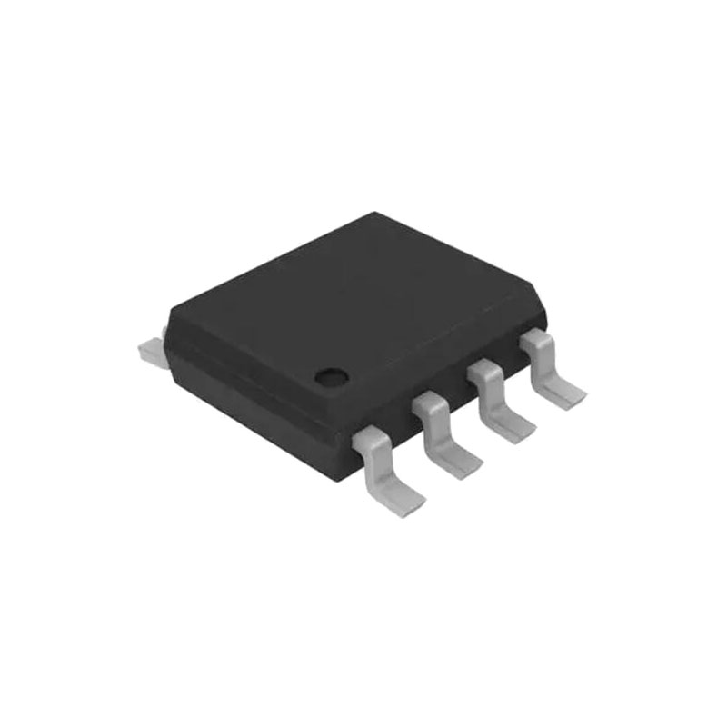
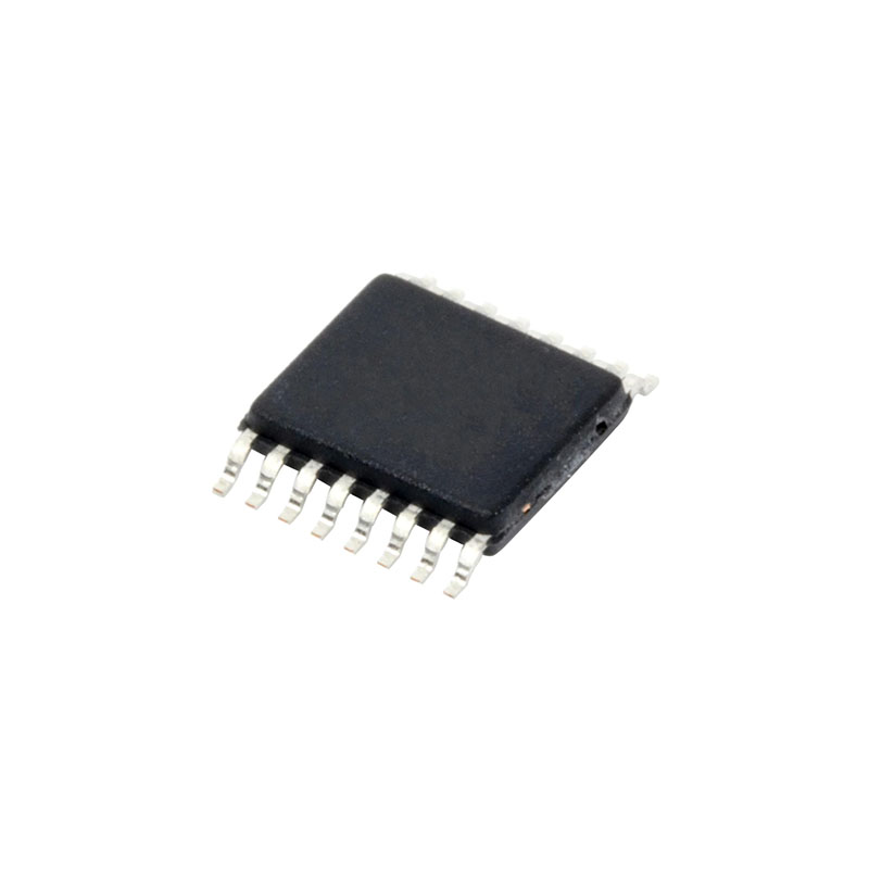
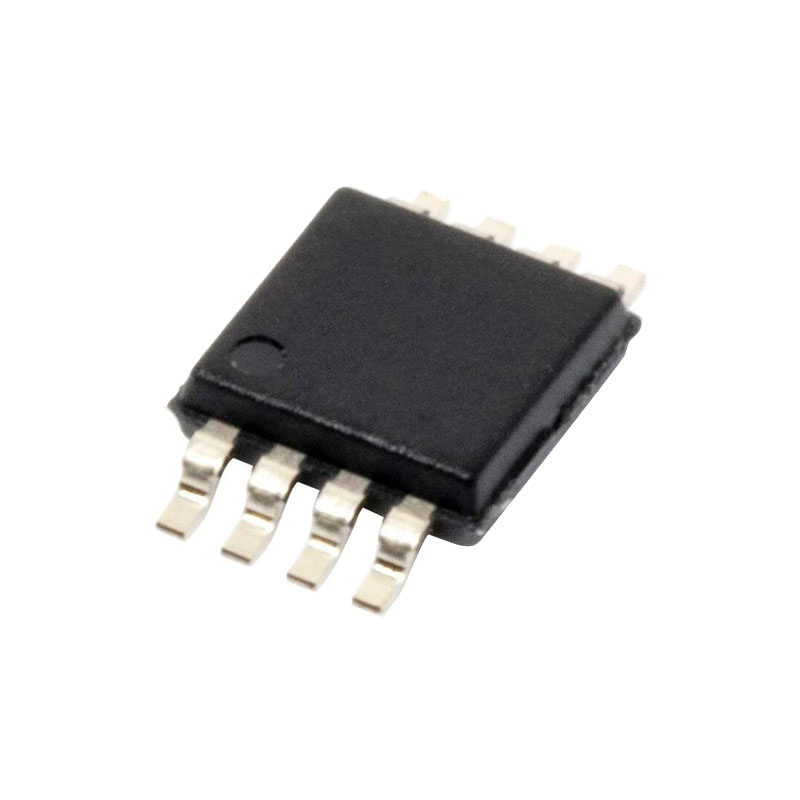
All electrical grades are available in an 8-lead SOIC package; the PDIP and TSSOP packages are available only in the lowest electrical grade.
FEATURES
Temperature coefficient: 5 ppm/°C maximum
High output current: 30 mA
Low supply current: 45 μA maximum
Initial accuracy: ±2 mV maximum1
Sleep mode: 15 μA maximum
Low dropout voltage
Load regulation: 4 ppm/mA
Line regulation: 4 ppm/V
Short-circuit protection
APPLICATIONS
Portable instruments
ADCs and DACs
Smart sensors
Solar powered applications
Loop-current-powered instruments
TEST PINS
Test Pin 1 and Test Pin 5 are reserved for in-package Zener zap. To achieve the highest level of accuracy at the output, the Zener zapping technique is used to trim the output voltage. Because each unit may require a different amount of adjustment, the resistance value at the test pins varies widely from pin to pin and from part to part.
ABSOLUTE MAXIMUM RATINGS
Stresses above those listed under Absolute Maximum Ratings may cause permanent damage to the device. This is a stress rating only; functional operation of the device at these or any other conditions above those indicated in the operational section of this specification is not implied. Exposure to absolute maximum rating conditions for extended periods may affect device reliability.
DEVICE POWER DISSIPATION CONSIDERATIONS
The REF19x family of references is capable of delivering load currents to 30 mA with an input voltage that ranges from 3.3 V to 15 V. When these devices are used in applications with large input voltages, exercise care to avoid exceeding the maximum internal power dissipation of these devices. Exceeding the published specifications for maximum power dissipation or junction temperature can result in premature device failure.
OUTPUT VOLTAGE BYPASSING
For stable operation, low dropout voltage regulators and references generally require a bypass capacitor connected from their VOUT pins to their GND pins. Although the REF19x family of references is capable of stable operation with capacitive loads exceeding 100 μF, a 1 μF capacitor is sufficient to guarantee rated performance.
The addition of a 0.1 μF ceramic capacitor in parallel with the bypass capacitor improves load current transient performance. For best line voltage transient performance, it is recommended that the voltage inputs of these devices be bypassed with a 10 μF electrolytic capacitor in parallel with a 0.1 μF ceramic capacitor.
SWITCHED OUTPUT 5 V/3.3 V
Applications often require digital control of reference voltages, selecting between one stable voltage and a second. With the sleep feature inherent to the REF19x series, switched output reference configurations are easily implemented with little additional hardware.
Which takes advantage of the output wire-OR capability of the REF19x device family. When off, a REF19x device is effectively an open circuit at the output node with respect to the power supply. When on, a REF19x device can source current up to its current rating, but sink only a few μA (essentially, just the relatively low current of the internal output scaling divider). Consequently, when two devices are wired together at their common outputs, the output voltage is the same as the output voltage for the on device. The off state device draws a small standby current of 15 μA (maximum), but otherwise does not interfere with operation of the on device, which can operate to its full current rating. Note that the two devices in the circuit conveniently share both input and output capacitors, and with CMOS logic drive, it is power efficient.

