Description
The SN65LBC175 and SN75LBC175 are monolithic, quadruple, differential line receivers with 3-state outputs designed to meet the requirements of the EIA standards RS-422-A, RS-423-A, RS-485, and CCITT Recommendation V.11. The devices are optimized for balanced multipoint bus transmission at data rates up to and exceeding 10 million bits per second. The receivers are enabled in pairs, with an active-high enable input. Each differential receiver input features high impedance, hysteresis for increased noise immunity, and sensitivity of ±200 mV over a common mode input voltage range of 12 V to −7 V. The failsafe design ensures that when the inputs are open-circuited, the outputs are always high. Both devices are designed using the TI proprietary LinBiCMOS™ technology, allowing low power consumption, high switching speeds, and robustness.
These devices offer optimum performance when used with the SN75LBC172 or SN75LBC174 quadruple-line drivers.
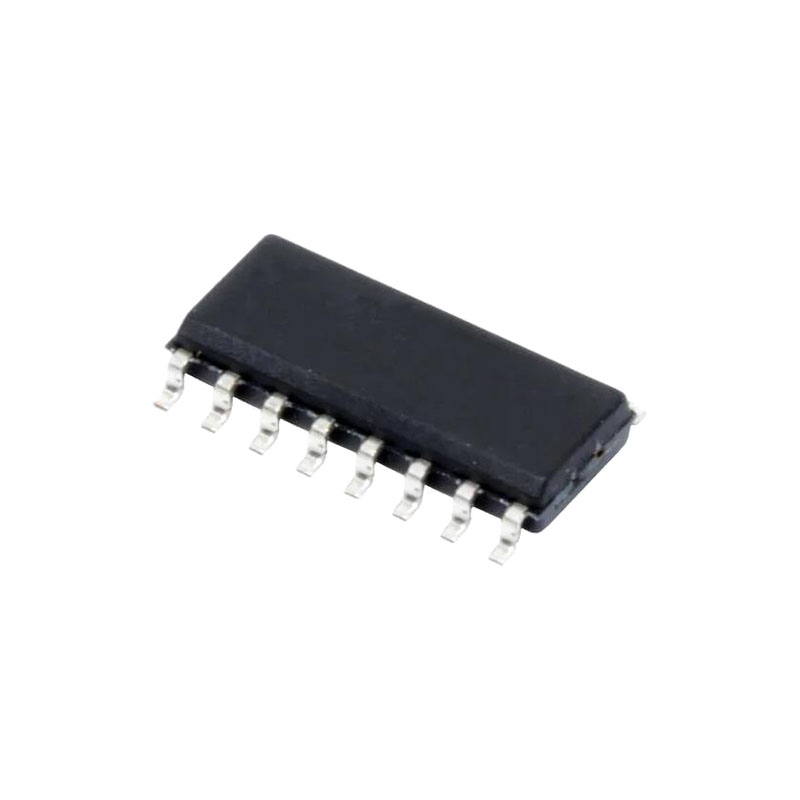
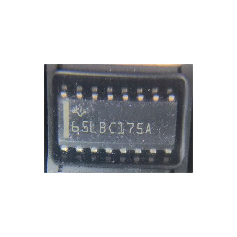
The SN65LBC175 is available in the 16-pin DIP (N), small-outline package (D), and the wide small-outline package (DW). The SN75LBC175 is available in the 16-pin DIP (N) and the small-outline package (D). The SN65LBC175 is characterized over the industrial temperature range of −40°C to 85°C. The SN75LBC175 is characterized for operation over the commercial temperature range of 0°C to 70°C.
Features
- Meets or exceeds the EIA standards RS-422-A, RS-423-A, RS-485, and CCITT recommendation V.11
- Designed to operate with pulse durations as short as 20 ns
- Designed for multipoint transmission on long bus lines in noisy environments
- Input sensitivity: ±200 mV
- Low-power consumption: 20 mA maximum
- Open-circuit fail-safe design
- Common-mode input voltage range of −7 V to 12 V
- Pin compatible with SN75175 and LTC489
Applications
- Factory automation
- ATM and cash counters
- Smart grid
- AC and servo motor drives
Electrostatic Discharge Caution
This integrated circuit can be damaged by ESD. Texas Instruments recommends that all integrated circuits be handled with appropriate precautions. Failure to observe proper handling and installation procedures can cause damage. ESD damage can range from subtle performance degradation to complete device failure. Precision integrated circuits may be more susceptible to damage because very small parametric changes could cause the device not to meet its published specifications.
Absolute Maximum Ratings: over operating free-air temperature range (unless otherwise noted)
| MIN | MAX | UNIT | |||
| VCC (see (2)) | Supply voltage range | -0.3 | 7 | V | |
| VI | Input voltage | (A or B inputs) | ±25 | V | |
| VID (see (3)) | Differential input voltage | ±25 | V | ||
| Voltage range at Y, 1/2EN, 3/4EN | -0.3 | VCC + 0.5 | V | ||
| Continuous total dissipation | See Dissipation Rating Table | ||||
| TA | Operating free-air temperature range: | SN65LBC175 | -40 | 85 | ℃ |
| SN75LBC175 | 0 | 70 | ℃ | ||
| Testing | Storage temperature range | -65 | 150 | ℃ | |
(1) Stresses beyond those listed under “absolute maximum ratings” may cause permanent damage to the device. These are stress ratings only, and functional operation of the device at these or any other conditions beyond those indicated under “recommended operating conditions” is not implied. Exposure to absolute maximum-rated conditions for extended periods may affect device reliability.
(2) All voltage values are concerning GND.
(3) Differential input voltage is measured at the noninverting input concerning the corresponding inverting input.
ESD Ratings
| VALUE | UNIT | ||
| V (ESD) Electrostatic discharge | Human-body model (HBM), per ANSI/ESDA/JEDEC JS-001(1) | ±1000 | V |
| Charged device model (CDM), per ANSI/ESDA/JEDEC JS-002(2) | ±1500 | ||
| Machine Model (MM) | ±200 |
(1)JEDEC document JEP155 states that 500-V HBM allows safe manufacturing with a standard ESD control process.
(2) JEDEC document JEP157 states that 250-V CDM allows safe manufacturing with a standard ESD control process. over an operating free-air temperature range (unless otherwise noted).
TEST CIRCUIT
A. The input pulse is supplied by a generator having the following characteristics: PRR = 1 MHz, duty cycle = 50%, t ≤ 6 ns, t ≤ Zo = 50Ω
B. CL includes probe and jig capacitance.
C. All diodes are 1N916 or equivalent.

