Описание:
The Cypress CY14B104M combines a 4-Mbit nonvolatile static RAM (nvSRAM) with a full-featured RTC in a monolithic integrated circuit. The embedded nonvolatile elements incorporate QuantumTrap technology, producing the world’s most reliable nonvolatile memory. The SRAM is read and written an infinite number of times, while independent nonvolatile data resides in the nonvolatile elements.
The RTC function provides an accurate clock with leap year tracking and a programmable, high-accuracy oscillator. The alarm function is programmable for periodic minutes, hours, days, or months alarms. There is also a programmable watchdog timer for process control.
The CY14B104M nvSRAM comprises two functional components paired in the same physical cell. These are an SRAM memory cell and a nonvolatile QuantumTrap cell. The SRAM memory cell operates as a standard fast static RAM. Data in the SRAM is transferred to the nonvolatile cell (the STORE operation) or from the nonvolatile cell to the SRAM (the RECALL operation). Using this unique architecture, all cells are stored and recalled in parallel. SRAM read and write operations are inhibited during the STORE and RECALL operations. The CY14B104M supports infinite reads and writes similar to a typical SRAM. In addition, it provides infinite RECALL operations from the nonvolatile cells and up to 1 million STORE operations.
Особенности:
■ 25 ns and 45 ns access times
■ Internally organized as 256 K × 16
■ Hands-off automatic STORE on power-down with only a small capacitor
■ STORE to QuantumTrap nonvolatile elements is initiated by software, device pin, or AutoStore on power-down.
■ RECALL to SRAM is initiated by software or power-up.
■ High reliability
■ Infinite read, write, and RECALL cycles
■ 1 million STORE cycles to QuantumTrap
■ 20-year data retention
■ Single 3 V +20%, –10% operation
■ Data integrity of Cypress nvSRAM combined with a full-featured real-time clock (RTC)
■ Watchdog timer
■ Clock alarm with programmable interrupts
■ Capacitor or battery backup for RTC
■ Industrial temperature
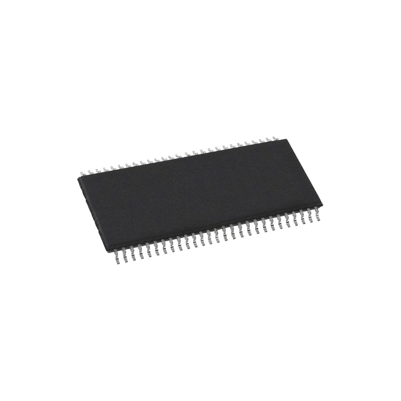
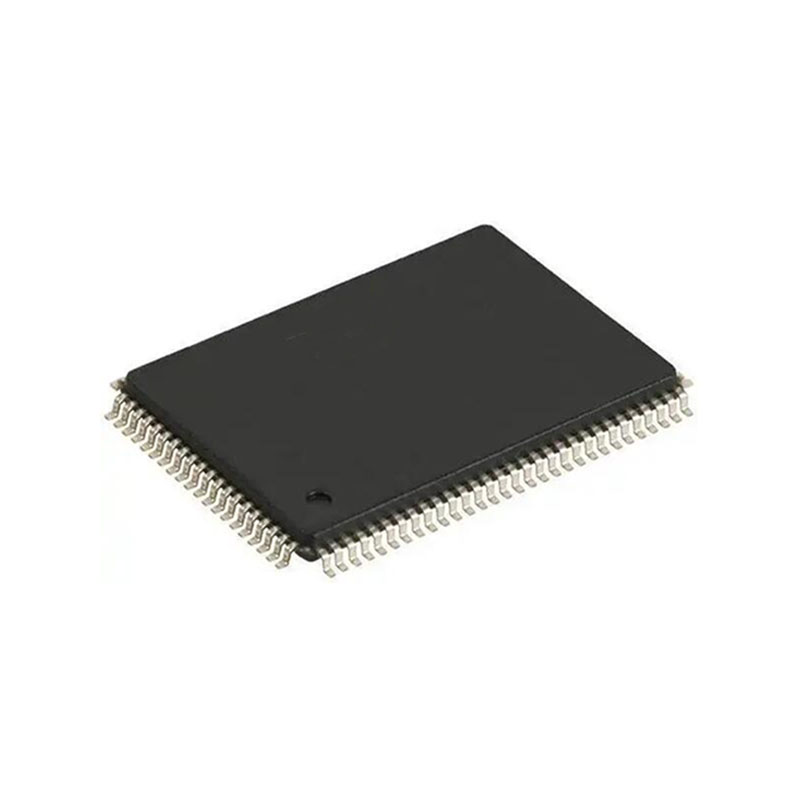
■ 44-pin and 54-pin thin small outline package (TSOP) Type II
■ Pb-free and restriction of hazardous substances (RoHS) compliant
Device Operation
The CY14B104K/CY14B104M nvSRAM is made up of two functional components paired in the same physical cell. These are an SRAM memory cell and a nonvolatile QuantumTrap cell. The SRAM memory cell operates as a standard fast static RAM. Data in the SRAM is transferred to the nonvolatile cell (the STORE operation), or from the nonvolatile cell to the SRAM (the RECALL operation). Using this unique architecture, all cells are stored and recalled in parallel. SRAM read and write operations are inhibited during the STORE and RECALL operations. The CY14B104K/CY14B104M supports infinite reads and writes similar to a typical SRAM. In addition, it provides infinite RECALL operations from the nonvolatile cells and up to 1 million STORE operations. See Truth Table For SRAM Operations on page 25 for a complete description of read and write modes.
SRAM Read
The CY14B104K/CY14B104M performs a read cycle when CE and OE are LOW and WE and HSB are HIGH. The address specified on pins A0–18 or A0–17 determines which of the 524,288 data bytes or 262,144 words of 16 bits each are accessed. Byte enables (BHE, BLE) determine which bytes are enabled to the output in the case of 16-bit words. When the read is initiated by an address transition, the outputs are valid after a delay of tAA (read cycle 1). If the read is initiated by CE or OE, the outputs are valid at tACE or at tDOE, whichever is later (read cycle 2). The data output repeatedly responds to address changes within the tAA access time without the need for transitions on any control input pins. This remains valid until another address change or until CE or OE is brought HIGH or WE or HSB is brought LOW.
SRAM Write
A write cycle is performed when CE and WE are LOW and HSB is HIGH. The address inputs must be stable before entering the write cycle and must remain stable until CE or WE go HIGH at the end of the cycle. The data on the common I/O pins DO0–15 are written into the memory if it is valid tSD before the end of a WE-controlled write or before the end of a CE-controlled write. The Byte Enable inputs (BHE, BLE) determine which bytes are written, in the case of 16-bit words. It is recommended that OE be kept HIGH during the entire write cycle to avoid data bus contention on common I/O lines. If OE is left LOW, internal circuitry turns off the output buffers tHZWE after WE go LOW.

