ОСОБЕННОСТИ
Very low voltage noise: 1 nV/√Hz maximum at 100 Hz
Excellent current gain match: 0.5%
Low offset voltage (VOS): 200 μV maximum (SOIC)
Outstanding offset voltage drift: 0.03 μV/°C
High gain bandwidth product: 200 MHz
ОБЩЕЕ ОПИСАНИЕ
The SSM2212 is a dual, NPN-matched transistor pair that is specifically designed to meet the requirements of ultralow noise audio systems.
With its extremely low input base spreading resistance (rbb’ is typically 28 Ω) and high current gain (hFE typically exceeds 600 at IC = 1 mA), the SSM2212 can achieve outstanding signal-to-noise ratios. The high current gain results in superior performance compared to systems incorporating commercially available monolithic amplifiers.
Excellent matching of the current gain (ΔhFE) to approximately 0.5% and low VOS of less than 10 μV typical make the SSM2212 ideal for symmetrically balanced designs, which reduce highorder amplifier harmonic distortion.
Stability of the matching parameters is guaranteed by protection diodes across the base-emitter junction. These diodes prevent degradation of beta and matching characteristics due to reverse biasing of the base-emitter junction.
The SSM2212 is also an ideal choice for accurate and reliable current biasing and mirroring circuits. Furthermore, because the accuracy of a current mirror degrades exponentially with mismatches of VBE between transistor pairs, the low VOS of the SSM2212 does not need offset trimming in most circuit applications.
The SSM2212 SOIC performance and characteristics are guaranteed over the extended temperature range of −40°C to +85°C.
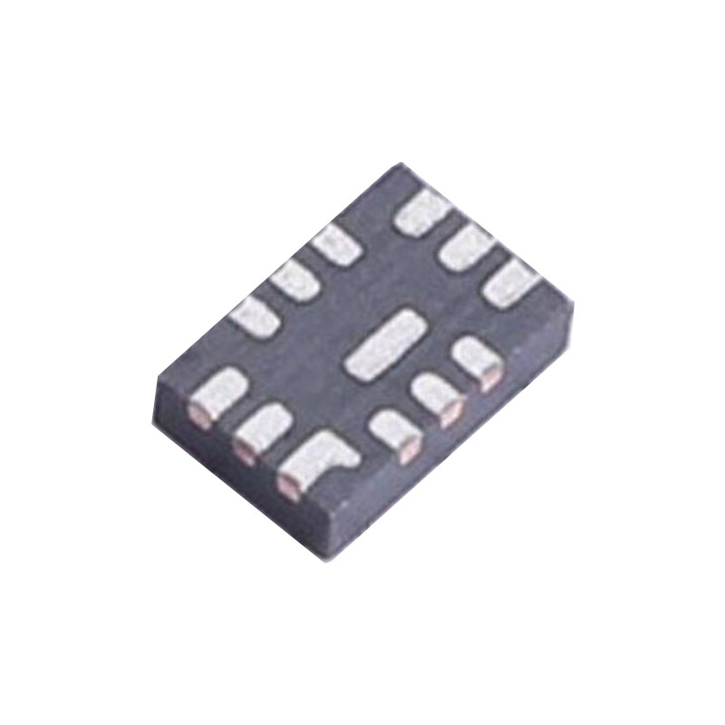
The SSM2212 is available in 8-lead SOIC and 16-lead LFCSP packages.
ABSOLUTE MAXIMUM RATING
Stresses at or above those listed under Absolute Maximum Ratings may cause permanent damage to the product. This is a stress rating only; functional operation of the product at these or any other conditions above those indicated in the operational section of this specification is not implied. Operation beyond
the maximum operating conditions for extended periods may affect product reliability.
ABSOLUTE MAXIMUM RATING
Stresses at or above those listed under Absolute Maximum Ratings may cause permanent damage to the product. This is a stress rating only; functional operation of the product at these or any other conditions above those indicated in the operational section of this specification is not implied. Operation beyond the maximum operating conditions for extended periods may affect product reliability.
ОСТОРОЖНО, ЭЛЕКТРОСТАТИЧЕСКОЕ РАЗРЯЖЕНИЕ
ESD(electrostatic discharge)sensitive device.Charged devices and circuit boards can discharge without detection. Although this product features patented or proprietary protection circuitry, damage may occur on devices subjected to high energy ESD.Therefore, proper ESD precautions should be taken to avoid performance degradation or loss of functionality.